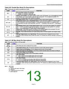
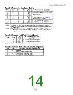
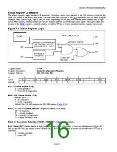
DS3251/DS3252/DS3253/DS3254
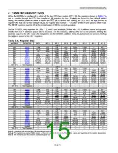
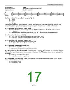
Register Name:
TCRn
Register Description:
Register Address:
Transmitter Configuration Register
01h, 11h, 21h, 31h
Bit
7
6
5
4
3
2
1
0
Name
Default
JAL[1]
0
TBIN
0
TCINV
0
TJA
0
TPD
0
TTS
1
TLBO
0
JAL[0]
0
Bits 7 and 0: Jitter Attenuator Buffer Length (JAL[1:0])
00 = 16 bits
01 = 32 bits
10 = 64 bits
11 = 128 bits
These lengths are the total size of the buffer. The jitter attenuator control logic seeks to keep the read and write
pointers half a buffer apart. Therefore typical latency through the jitter attenuator is half the buffer length.
Bit 6: Transmitter Binary Interface Enable (TBIN)
0 = Transmitter framer interface is bipolar on the TPOS and TNEG pins. The B3ZS/HDB3 encoder is
disabled.
1 = Transmitter framer interface is binary on the TDAT pin. The B3ZS/HDB3 encoder is enabled.
Bit 5: Transmitter Clock Invert (TCINV)
0 = TPOS/TDAT and TNEG are sampled on the rising edge of TCLK.
1 = TPOS/TDAT and TNEG are sampled on the falling edge of TCLK.
Bit 4: Transmitter Jitter Attenuator Enable (TJA)
0 = Remove jitter attenuator from the transmitter path.
1 = Insert jitter attenuator into the transmitter path.
Bit 3: Transmitter Power-Down Enable (TPD)
0 = enable the transmitter
1 = power-down the transmitter (output driver tri-stated)
Bit 2: Transmitter Tri-State Enable (TTS). This bit is set to 1 on reset, which tri-states the transmitter TXP and
TXN pins. The transmitter circuitry is left powered up in this mode. The TTS input pin is inverted and logically ORed
with this bit.
0 = enable the transmitter output driver
1 = tri-state the transmitter output driver
Bit 1: Transmitter Line Build-Out (TLBO). TLBO indicates cable length for waveform shaping in DS3 and STS-1
modes. TLBO is ignored in E3 mode.
0 = cable length O 225ft
1 = cable length < 225ft
17 of 71

 DALLAS [ DALLAS SEMICONDUCTOR ]