DS3251/DS3252/DS3253/DS3254
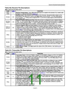
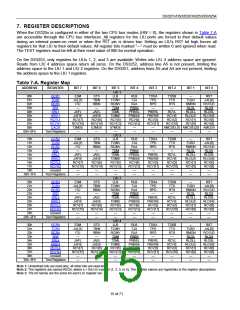
Table 6-B. Receiver Pin Descriptions
Note: These pins are always active.
NAME
TYPE
FUNCTION
RXPn,
Receiver Analog Inputs. These differential AMI inputs are coupled to the inbound 75ꢀ coaxial cable
I
RXNn
through a 1:2 step-up transformer (Figure 2-1).
Receiver Clock. The recovered clock is output on the RCLK pin. Recovered data is output on the
RPOS/RDAT and RNEG/RLCV pins on the falling edge of RCLK (RCINV = 0) or the rising edge of
RCLK (RCINV = 1). During a loss of signal (RLOS = 0), the RCLK output signal is derived from the
LIU’s master clock.
RCLKn
O3
O3
Receiver Positive AMI/Receiver Data. When the receiver is configured to have a bipolar interface
(RBIN = 0), RPOS pulses high for each positive AMI pulse received. When the receiver is configured
to have a binary interface (RBIN = 1), RDAT outputs decoded binary data. RPOS/RDAT is updated
either on the falling edge of RCLK (RCINV = 0) or the rising edge of RCLK (RCINV = 1).
RPOSn/
RDATn
Receiver Negative AMI/Line-Code Violation. When the receiver is configured to have a bipolar
interface (RBIN = 0), RNEG pulses high for each negative AMI pulse received. When the receiver is
configured to have a binary interface (RBIN = 1), RLCV pulses high to flag code violations. See
Section 8.6 for further details on code violations. RNEG/RLCV is updated either on the falling edge of
RCLK (RCINV = 0) or the rising edge of RCLK (RCINV = 1).
RNEGn/
RLCVn
O3
I
Receiver Tri-State Enable (Active Low). RTS tri-states the RPOS/RDAT, RNEG/RLCV, and RCLK
receiver outputs. This feature supports applications requiring LIU redundancy. Receiver outputs from
multiple LIUs can be wire-ORed together, eliminating the need for external switches or muxes. The
receiver continues to operate internally when RTS is low.
RTSn
0 = tri-state the receiver outputs
1 = enable the receiver outputs
Receiver Loss of Signal (Active Low, Open Drain). RLOS is asserted upon detection of 175 M75
consecutive zeros in the receive data stream. RLOS is deasserted when there are no excessive zero
occurrences over a span of 175 M75 clock periods. An excessive zero occurrence is defined as three
or more consecutive zeros in the DS3 and STS-1 modes or four or more zeros in the E3 mode. See
Section 8.5 for more information.
O
O
RLOSn
PRBS Detector Output. This signal reports the status of the PRBS detector. See Section 11 for
PRBSn
further details.
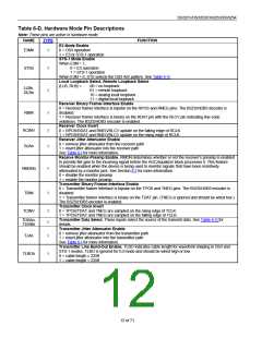
Table 6-C. Transmitter Pin Descriptions
Note: These pins are always active.
NAME
TYPE
FUNCTION
Transmitter Clock. A DS3 (44.736MHz M20ppm), E3 (34.368MHz M20ppm), or STS-1 (51.840MHz
M20ppm) clock should be applied at this signal. Data to be transmitted is clocked into the device at
TPOS/TDAT and TNEG either on the rising edge of TCLK (TCINV = 0) or the falling edge of TCLK
(TCINV = 1). See Section 9 for additional details.
TCLKn
I
Transmitter Positive AMI/Transmitter Data. When the transmitter is configured to have a bipolar
interface (TBIN = 0), a positive pulse is transmitted on the line when TPOS is high. When the
transmitter is configured to have a binary interface (TBIN = 1), the data on TDAT is transmitted after
B3ZS or HDB3 encoding. TPOS/TDAT is sampled either on the rising edge of TCLK (TCINV = 0) or
on the falling edge of TCLK (TCINV = 1).
TPOSn/
TDATn
I
I
Transmitter Negative AMI. When the transmitter is configured to have a bipolar interface (TBIN = 0),
a negative pulse is transmitted on the line when TNEG is high. When the transmitter is configured to
have a binary interface (TBIN = 1), TNEG is ignored and should be wired either high or low. TNEG is
sampled either on the rising edge of TCLK (TCINV = 0) or on the falling edge of TCLK (TCINV = 1).
Transmitter Analog Outputs. These differential AMI outputs are coupled to the outbound 75ꢀ
coaxial cable through a 2:1 step-down transformer (Figure 2-1). These outputs can be tri-stated using
the TTS pin or the TTS or TPS configuration bits.
TNEGn
TXPn,
TXNn
O3
O
Transmitter Driver Monitor (Active Low, Open Drain). TDM reports the status of the transmit driver
monitor. When the monitor detects a faulty transmitter, TDM is driven low. TDM requires an external
pullup to VDD. See Section 9.6 for more information.
TDMn
Transmitter Tri-State Enable (Active Low). TTS tri-states the transmitter outputs (TXP and TXN).
This feature supports applications requiring LIU redundancy. Transmitter outputs from multiple LIUs
can be wire-ORed together, eliminating external switches. The transmitter continues to operate
internally when TTS is active.
TTSn
I
0 = tri-state the transmitter output driver
1 = enable the transmitter output driver
11 of 71

 DALLAS [ DALLAS SEMICONDUCTOR ]