DS3251/DS3252/DS3253/DS3254
6. PIN DESCRIPTIONS
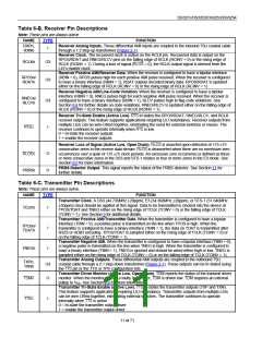
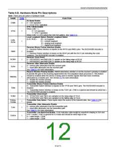
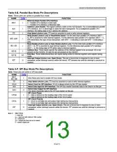
Table 6-A through Table 6-C list the pins that are always active. Table 6-D through Table 6-F list the additional pins
that active in each of the three control interface modes. Section 18 shows pin assignments for all three control
interface modes.
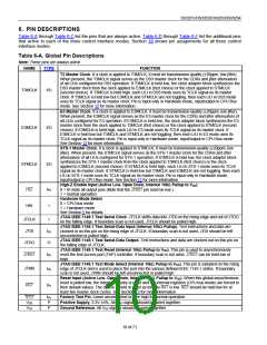
Table 6-A. Global Pin Descriptions
Note: These pins are always active.
NAME
TYPE
FUNCTION
T3 Master Clock. If a clock is applied to T3MCLK, it must be transmission-quality (M20ppm, low jitter).
When present, the T3MCLK signal serves as the DS3 master clock for the CDRs and jitter attenuators
of all LIUs configured for DS3 operation. If T3MCLK is held low, the clock adapter block synthesizes the
DS3 master clock from the clock applied to E3MCLK (first choice) or the clock applied to STMCLK
(second choice). If T3MCLK is held high, each LIU in DS3 mode uses its TCLK signal as its master
clock. If T3MCLK is held low but E3MCLK and STMCLK are not toggling, then each LIU in DS3 mode
uses its TCLK signal as its master clock. Pin is input-only in Hardware mode, input/output in CPU Bus
mode. See Section 12 for more information.
T3MCLK
I/O
E3 Master Clock. If a clock is applied to E3MCLK, it must be transmission-quality (M20ppm, low jitter).
When present, the E3MCLK signal serves as the E3 master clock for the CDRs and jitter attenuators of
all LIUs configured for E3 operation. If E3MCLK is held low, the clock adapter block synthesizes the E3
master clock from the clock applied to T3MCLK (first choice) or the clock applied to STMCLK (second
choice). If E3MCLK is held high, each LIU in E3 mode uses its TCLK signal as its master clock. If
E3MCLK is held low but T3MCLK and STMCLK are not toggling, then each LIU in E3 mode uses its
TCLK signal as its master clock. Pin is input-only in Hardware mode, input/output in CPU Bus mode.
See Section 12 for more information.
STS-1 Master Clock. If a clock is applied to STMCLK, it must be transmission-quality (M20ppm, low
jitter). When present, the STMCLK signal serves as the STS-1 master clock for the CDRs and jitter
attenuators of all LIUs configured for STS-1 operation. If STMCLK is held low, the clock adapter block
synthesizes the STS-1 master clock from the clock applied to T3MCLK (first choice) or the clock
applied to E3MCLK (second choice). If STMCLK is held high, each LIU in STS-1 mode uses its TCLK
signal as its master clock. If STMCLK is held low but T3MCLK and E3MCLK are not toggling, then each
LIU in STS-1 mode uses its TCLK signal as its master clock. Pin is input-only in Hardware mode,
input/output in CPU Bus mode. See Section 12 for more information.
E3MCLK
STMCLK
I/O
I/O
High-Z Enable Input (Active Low, Open Drain, Internal 10kꢀ Pullup to VDD
0 = tri-state all output pins (Note that the JTRST pin must be low.)
1 = normal operation
)
HIZ
IPU
Hardware Mode Select
0 = CPU bus mode
HW
I
1 = Hardware mode
See Section 5 for details.
JTAG IEEE 1149.1 Test Serial Clock. JTCLK shifts data into JTDI on the rising edge and out of JTDO
on the falling edge. If boundary scan is not used, JTCLK should be pulled high.
JTAG IEEE 1149.1 Test Serial-Data Input (Internal 10kꢀ Pullup). Test instructions and data are
clocked in on this pin on the rising edge of JTCLK. If boundary scan is not used, JTDI should be left
unconnected or pulled high.
JTCLK
JTDI
I
IPU
O
JTAG IEEE 1149.1 Test Serial-Data Output. Test instructions and data are clocked out on this pin on
the falling edge of JTCLK.
JTDO
JTRST
JTAG IEEE 1149.1 Test Reset (Internal 10kꢀ Pullup to VDD). This pin is used to asynchronously
reset the test access port (TAP) controller. If boundary scan is not used, JTRST can be held low or
high.
IPU
JTAG IEEE 1149.1 Test Mode Select (Internal 10kꢀ Pullup to VDD). This pin is sampled on the rising
edge of JTCLK and is used to place the port into the various defined IEEE 1149.1 states. If boundary
scan is not used, JTMS should be left unconnected or pulled high.
JTMS
IPU
Reset Input (Active Low, Open Drain, Internal 10kꢀ Pullup to VDD). When this global asynchronous
reset is pulled low, the internal circuitry is reset and the internal registers (CPU bus mode) are forced to
their default values. The device is held in reset as long as RST is low. RST should be held low for at
least two master clock cycles. See Section 13 for more information.
RST
IPU
Factory Test Pin. Leave unconnected or wire high for normal operation.
IPU
P
P
TEST
VDD
VSS
Positive Supply. 3.3V M5%. All VDD signals should be wired together.
Ground Reference. All VSS signals should be wired together.
10 of 71

 DALLAS [ DALLAS SEMICONDUCTOR ]