DS3251/DS3252/DS3253/DS3254
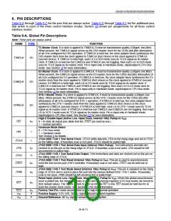
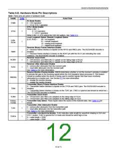
Table 6-D. Hardware Mode Pin Descriptions
Note: These pins are active in hardware mode.
NAME
TYPE
FUNCTION
E3 Mode Enable
E3Mn
I
0 = DS3 operation
1 = E3 or STS-1 operation
STS-1 Mode Enable
When E3M = 1,
STSn
I
I
I
0 = E3 operation
1 = STS-1 operation
When E3M = 0, STS selects the DS3 AIS pattern. See Table 6-G.
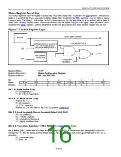
Local Loopback Select, Remote Loopback Select
{LLB, RLB} =
00 = no loopback
LLBn,
RLBn
01 = remote loopback
10 = analog local loopback
11 = digital local loopback
Receiver Binary Framer-Interface Enable
0 = Receiver framer interface is bipolar on the RPOS and RNEG pins. The B3ZS/HDB3 decoder is
disabled.
RBIN
1 = Receiver framer interface is binary on the RDAT pin with the RLCV pin indicating line-code
violations. The B3ZS/HDB3 encoder is enabled.
Receiver Clock Invert
RCINV
RJAn
I
I
0 = RPOS/RDAT and RNEG/RLCV update on the falling edge of RCLK.
1 = RPOS/RDAT and RNEG/RLCV update on the rising edge of RCLK.
Receiver Jitter Attenuator Enable
0 = remove jitter attenuator from the receiver path
1 = insert jitter attenuator into the receiver path
See Table 6-I for more information.
Receive Monitor-Preamp Enable. RMON determines whether or not the receiver’s preamp is enabled
to provide flat gain to the incoming signal before the AGC/equalizer block processes it. This feature
should be enabled when the device is being used to monitor signals that have been resistively
attenuated by a monitor jack. See Section 8.2 for more information.
0 = disable the monitor preamp
RMONn
I
I
1 = enable the monitor preamp
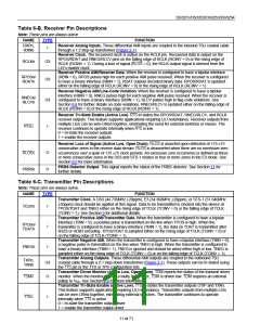
Transmitter Binary Framer-Interface Enable
0 = Transmitter framer interface is bipolar on the TPOS and TNEG pins. The B3ZS/HDB3 encoder is
disabled.
TBIN
1 = Transmitter framer interface is binary on the TDAT pin. (TNEG is ignored and should be wired low.)
The B3ZS/HDB3 encoder is enabled.
Transmitter Clock Invert
TCINV
I
I
0 = TPOS/TDAT and TNEG are sampled on the rising edge of TCLK.
1 = TPOS/TDAT and TNEG are sampled on the falling edge of TCLK.
Transmitter Data Select. These inputs select the source of the transmit data. See Table 6-G for
details.
TDSAn,
TDSBn
Transmitter Jitter Attenuator Enable
0 = remove jitter attenuator from the transmitter path
1 = insert jitter attenuator into the transmitter path
TJAn
I
I
See Table 6-I for more information.
Transmitter Line Build-Out Enable. TLBO indicates cable length for waveform shaping in DS3 and
STS-1 modes. TLBO is ignored for E3 mode and should be wired high or low.
0 = cable length O 225ft
TLBOn
1 = cable length < 225ft
12 of 71

 DALLAS [ DALLAS SEMICONDUCTOR ]