PSoC® 3: CY8C32 Family
Data Sheet
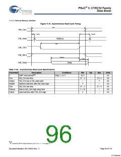
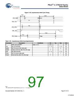
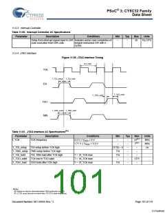
Figure 11-52. Asynchronous Write Cycle Timing
Taddrv
Taddrh
EM_Addr
EM_CEn
Address
Tcel
Twel
EM_WEn
EM_OEn
Tdweh
Tdcev
EM_Data
Data
Table 11-53. Asynchronous Write Cycle Specifications
Parameter
T
Description
EMIF clock period[43]
Conditions
Min
30.3
T – 5
–
Typ
–
Max
Units
nS
Vdda ≥ 3.3 V
–
Tcel
EM_CEn low time
–
T + 5
nS
Taddrv
Taddrh
Twel
EM_CEn low to EM_Addr valid
Address hold time after EM_WEn high
EM_WEn low time
–
5
–
nS
T
–
nS
T – 5
–
–
T + 5
7
nS
Tdcev
Tdweh
EM_CEn low to data valid
Data hold time after EM_WEn high
–
nS
T
–
–
nS
Note
43. Limited by GPIO output frequency, see Table 11-10 on page 72.
Document Number: 001-56955 Rev. *J
Page 97 of 119
[+] Feedback

 CYPRESS [ CYPRESS ]