PSoC® 3: CY8C32 Family
Data Sheet
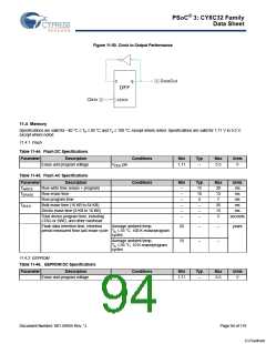
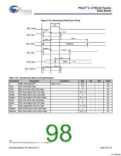
Figure 11-50. Clock to Output Performance
11.4 Memory
Specifications are valid for –40 °C ≤ TA ≤ 85 °C and TJ ≤ 100 °C, except where noted. Specifications are valid for 1.71 V to 5.5 V,
except where noted.
11.4.1 Flash
Table 11-44. Flash DC Specifications
Parameter
Description
Conditions
Conditions
Min
Typ
Max
Units
Erase and program voltage
V
DDD pin
1.71
–
5.5
V
Table 11-45. Flash AC Specifications
Parameter
TWRITE
Description
Row write time (erase + program)
Row erase time
Min
–
Typ
15
10
5
Max
20
13
7
Units
ms
TERASE
–
ms
Row program time
–
ms
TBULK
Bulk erase time (16 KB to 64 KB)
Sector erase time (8 KB to 16 KB)
–
–
35
15
5
ms
–
–
ms
Total device program time, including
JTAG or SWD, and other overhead
–
–
seconds
Flash data retention time, retention
period measured from last erase cycle TA ≤ 55 °C, 100 K erase/program
Average ambient temp.
20
10
–
–
–
–
years
cycles
Average ambient temp.
TA ≤ 85 °C, 10 K erase/program
cycles
11.4.2 EEPROM
Table 11-46. EEPROM DC Specifications
Parameter
Description
Conditions
Min
Typ
Max
Units
Erase and program voltage
1.71
–
5.5
V
Document Number: 001-56955 Rev. *J
Page 94 of 119
[+] Feedback

 CYPRESS [ CYPRESS ]