PSoC® 3: CY8C32 Family
Data Sheet
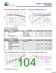
11.5 PSoC System Resources
Specifications are valid for –40 °C ≤ TA ≤ 85 °C and TJ ≤ 100 °C, except where noted. Specifications are valid for 1.71 V to 5.5 V,
except where noted.
11.5.1 POR with Brown Out
For brown out detect in regulated mode, VDDD and VDDA must be ≥ 2.0 V. Brown out detect is not available in externally regulated
mode.
Table 11-56. Precise Power-on Reset (PRES) with Brown Out DC Specifications
Parameter
Description
Precise POR (PPOR)
Conditions
Min
Typ
Max
Units
PRESR
PRESF
Rising trip voltage
Falling trip voltage
Factory trim
1.64
1.62
–
–
1.68
1.66
V
V
Table 11-57. Power-on Reset (POR) with Brown Out AC Specifications
Parameter
Description
Conditions
Min
–
Typ
–
Max
0.5
–
Units
µs
PRES_TR Response time
V
DDD/VDDA droop rate
Sleep mode
–
5
V/sec
11.5.2 Voltage Monitors
Table 11-58. Voltage Monitors DC Specifications
Parameter
Description
Conditions
Min
Typ
Max
Units
LVI
Trip voltage
LVI_A/D_SEL[3:0] = 0000b
LVI_A/D_SEL[3:0] = 0001b
LVI_A/D_SEL[3:0] = 0010b
LVI_A/D_SEL[3:0] = 0011b
LVI_A/D_SEL[3:0] = 0100b
LVI_A/D_SEL[3:0] = 0101b
LVI_A/D_SEL[3:0] = 0110b
LVI_A/D_SEL[3:0] = 0111b
LVI_A/D_SEL[3:0] = 1000b
LVI_A/D_SEL[3:0] = 1001b
LVI_A/D_SEL[3:0] = 1010b
LVI_A/D_SEL[3:0] = 1011b
LVI_A/D_SEL[3:0] = 1100b
LVI_A/D_SEL[3:0] = 1101b
LVI_A/D_SEL[3:0] = 1110b
LVI_A/D_SEL[3:0] = 1111b
Trip voltage
1.68
1.89
2.14
2.38
2.62
2.87
3.11
3.35
3.59
3.84
4.08
4.32
4.56
4.83
5.05
5.30
5.57
1.73
1.95
2.20
2.45
2.71
2.95
3.21
3.46
3.70
3.95
4.20
4.45
4.70
4.98
5.21
5.47
5.75
1.77
2.01
2.27
2.53
2.79
3.04
3.31
3.56
3.81
4.07
4.33
4.59
4.84
5.13
5.37
5.63
5.92
V
V
V
V
V
V
V
V
V
V
V
V
V
V
V
V
V
HVI
Table 11-59. Voltage Monitors AC Specifications
Parameter Description
Response time
Conditions
Min
Typ
Max
Units
–
–
1
µs
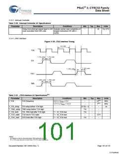
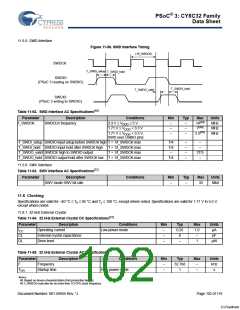
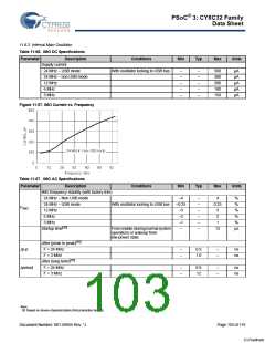
Document Number: 001-56955 Rev. *J
Page 100 of 119
[+] Feedback

 CYPRESS [ CYPRESS ]