PSoC® 3: CY8C32 Family
Data Sheet
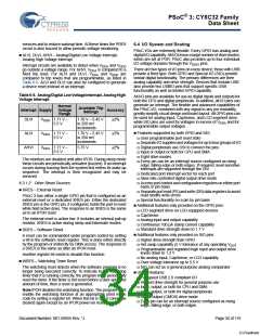
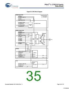
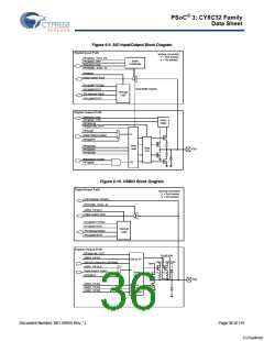
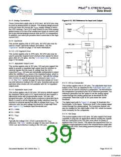
Figure 6-8. GPIO Block Diagram
Digital Input Path
Naming Convention
PRT[x]CTL
PRT[x]DBL_SYNC_IN
‘x’ = Port Number
‘y’ = Pin Number
PRT[x]PS
Digital System Input
PICU[x]INTTYPE[y]
PICU[x]INTSTAT
Pin Interrupt Signal
PICU[x]INTSTAT
Input Buffer Disable
Interrupt
Logic
Digital Output Path
PRT[x]SLW
PRT[x]SYNC_OUT
Vddio Vddio
PRT[x]DR
0
1
In
Digital System Output
PRT[x]BYP
Vddio
Drive
Logic
PRT[x]DM2
PRT[x]DM1
PRT[x]DM0
Slew
Cntl
PIN
Bidirectional Control
PRT[x]BIE
OE
Analog
1
0
1
0
1
Capsense Global Control
CAPS[x]CFG1
Switches
PRT[x]AG
Analog Global Enable
PRT[x]AMUX
Analog Mux Enable
LCD
Display
Data
Logic & MUX
PRT[x]LCD_COM_SEG
PRT[x]LCD_EN
LCD Bias Bus
5
Document Number: 001-56955 Rev. *J
Page 35 of 119
[+] Feedback

 CYPRESS [ CYPRESS ]