PSoC® 3: CY8C32 Family
Data Sheet
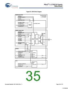
6.4.8 Analog Connections
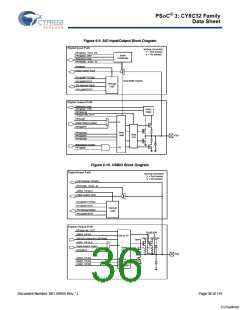
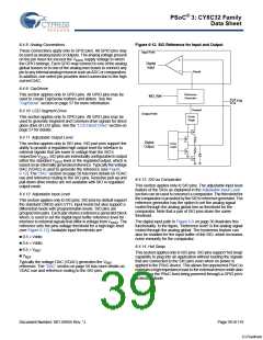
Figure 6-12. SIO Reference for Input and Output
These connections apply only to GPIO pins. All GPIO pins may
be used as analog inputs or outputs. The analog voltage present
on the pin must not exceed the VDDIO supply voltage to which
the GPIO belongs. Each GPIO may connect to one of the analog
global busses or to one of the analog mux buses to connect any
pin to any internal analog resource such as ADC or comparators.
In addition, one select pin provides direct connection to the high
current DAC.
Input Path
Digital
Input
Vinref
6.4.9 CapSense
Reference
Generator
This section applies only to GPIO pins. All GPIO pins may be
used to create CapSense buttons and sliders. See the
“CapSense” section on page 57 for more information.
SIO_Ref
PIN
Voutref
6.4.10 LCD Segment Drive
Output Path
Driver
Vhigh
This section applies only to GPIO pins. All GPIO pins may be
used to generate Segment and Common drive signals for direct
glass drive of LCD glass. See the “LCD Direct Drive” section on
page 57 for details.
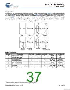
6.4.11 Adjustable Output Level
Digital
Output
Drive
Logic
This section applies only to SIO pins. SIO port pins support the
ability to provide a regulated high output level for interface to
external signals that are lower in voltage than the SIO’s
respective VDDIO. SIO pins are individually configurable to output
either the standard VDDIO level or the regulated output, which is
based on an internally generated reference. Typically the voltage
DAC (VDAC) is used to generate the reference (see Figure
6-12). The “DAC” section on page 58 has more details on VDAC
use and reference routing to the SIO pins. Resistive pull-up and
pull-down drive modes are not available with SIO in regulated
output mode.
6.4.13 SIO as Comparator
This section applies only to SIO pins. The adjustable input level
feature of the SIOs as explained in the Adjustable Input Level
section can be used to construct a comparator. The threshold for
the comparator is provided by the SIO's reference generator. The
reference generator has the option to set the analog signal
routed through the analog global line as threshold for the
comparator. Note that a pair of SIO pins share the same
threshold.
6.4.12 Adjustable Input Level
This section applies only to SIO pins. SIO pins by default support
the standard CMOS and LVTTL input levels but also support a
differential mode with programmable levels. SIO pins are
grouped into pairs. Each pair shares a reference generator block
which, is used to set the digital input buffer reference level for
interface to external signals that differ in voltage from VDDIO. The
reference sets the pins voltage threshold for a high logic level
(see Figure 6-12). Available input thresholds are:
The digital input path in Figure 6-9 on page 36 illustrates this
functionality. In the figure, ‘Reference level’ is the analog signal
routed through the analog global. The hysteresis feature can
also be enabled for the input buffer of the SIO, which increases
noise immunity for the comparator.
0.5 × Vddio
0.4 × Vddio
0.5 × VREF
VREF
6.4.14 Hot Swap
This section applies only to SIO pins. SIO pins support ‘hot swap’
capability to plug into an application without loading the signals
that are connected to the SIO pins even when no power is
applied to the PSoC device. This allows the unpowered PSoC to
maintain a high impedance load to the external device while also
preventing the PSoC from being powered through a GPIO pin’s
protection diode.
Typically the voltage DAC (VDAC) generates the VREF
reference. The “DAC” section on page 58 has more details on
VDAC use and reference routing to the SIO pins.
Document Number: 001-56955 Rev. *J
Page 39 of 119
[+] Feedback

 CYPRESS [ CYPRESS ]