PSoC® 3: CY8C32 Family
Data Sheet
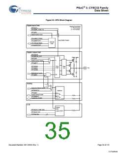
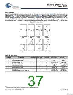
High Impedance Analog
6.4.3 Bidirectional Mode
The default reset state with both the output driver and digital
input buffer turned off. This prevents any current from flowing
in the I/O’s digital input buffer due to a floating voltage. This
state is recommended for pins that are floating or that support
an analog voltage. High impedance analog pins do not provide
digital input functionality.
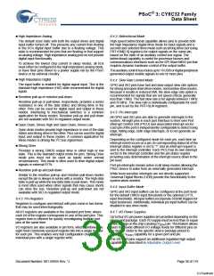
High-speed bidirectional capability allows pins to provide both
the high impedance digital drive mode for input signals and a
second user selected drive mode such as strong drive (set using
PRT×DM[2:0] registers) for output signals on the same pin,
based on the state of an auxiliary control bus signal. The
bidirectional capability is useful for processor busses and
communications interfaces such as the SPI Slave MISO pin that
requires dynamic hardware control of the output buffer.
To achieve the lowest chip current in sleep modes, all I/Os
must either be configured to the high impedance analog mode,
or have their pins driven to a power supply rail by the PSoC
device or by external circuitry.
The auxiliary control bus routes up to 16 UDB or digital peripheral
generated output enable signals to one or more pins.
High Impedance Digital
6.4.4 Slew Rate Limited Mode
The input buffer is enabled for digital signal input. This is the
standard high impedance (HiZ) state recommended for digital
inputs.
GPIO and SIO pins have fast and slow output slew rate options
for strong and open drain drive modes, not resistive drive modes.
Because it results in reduced EMI, the slow edge rate option is
recommended for signals that are not speed critical, generally
less than 1 MHz. The fast slew rate is for signals between 1 MHz
and 33 MHz. The slew rate is individually configurable for each
pin, and is set by the PRT×SLW registers.
Resistive pull-up or resistive pull-down
Resistive pull-up or pull-down, respectively, provides a series
resistance in one of the data states and strong drive in the
other. Pins can be used for digital input and output in these
modes. Interfacing to mechanical switches is a common
application for these modes. Resistive pull-up and pull-down
are not available with SIO in regulated output mode.
6.4.5 Pin Interrupts
All GPIO and SIO pins are able to generate interrupts to the
system. All eight pins in each port interface to their own Port
Interrupt Control Unit (PICU) and associated interrupt vector.
Each pin of the port is independently configurable to detect rising
edge, falling edge, both edge interrupts, or to not generate an
interrupt.
Open Drain, Drives High and Open Drain, Drives Low
Open drain modes provide high impedance in one of the data
states and strong drive in the other. Pins can be used for digital
input and output in these modes. A common application for
these modes is driving the I2C bus signal lines.
Depending on the configured mode for each pin, each time an
interrupt event occurs on a pin, its corresponding status bit of the
interrupt status register is set to “1” and an interrupt request is
sent to the interrupt controller. Each PICU has its own interrupt
vector in the interrupt controller and the pin status register
providing easy determination of the interrupt source down to the
pin level.
Strong Drive
Provides a strong CMOS output drive in either high or low
state. This is the standard output mode for pins. Strong Drive
mode pins must not be used as inputs under normal
circumstances. This mode is often used to drive digital output
signals or external FETs.
Port pin interrupts remain active in all sleep modes allowing the
PSoC device to wake from an externally generated interrupt.
Resistive pull-up and pull-down
While level sensitive interrupts are not directly supported;
Universal Digital Blocks (UDB) provide this functionality to the
system when needed.
Similar to the resistive pull-up and resistive pull-down modes
except the pin is always in series with a resistor. The high data
state is pull-up while the low data state is pull-down. This mode
is most often used when other signals that may cause shorts
can drive the bus. Resistive pull-up and pull-down are not
available with SIO in regulated output mode.
6.4.6 Input Buffer Mode
GPIO and SIO input buffers can be configured at the port level
for the default CMOS input thresholds or the optional LVTTL
input thresholds. All input buffers incorporate Schmitt triggers for
input hysteresis. Additionally, individual pin input buffers can be
disabled in any drive mode.
6.4.2 Pin Registers
Registers to configure and interact with pins come in two forms
that may be used interchangeably.
All I/O registers are available in the standard port form, where
each bit of the register corresponds to one of the port pins. This
register form is efficient for quickly reconfiguring multiple port
pins at the same time.
6.4.7 I/O Power Supplies
Up to four I/O pin power supplies are provided depending on the
device and package. Each I/O supply must be less than or equal
to the voltage on the chip’s analog (VDDA) pin. This feature allows
users to provide different I/O voltage levels for different pins on
the device. Refer to the specific device package pinout to
determine VDDIO capability for a given port and pin.
I/O registers are also available in pin form, which combines the
eight most commonly used port register bits into a single register
for each pin. This enables very fast configuration changes to
individual pins with a single register write.
The SIO port pins support an additional regulated high output
capability, as described in Adjustable Output Level.
Document Number: 001-56955 Rev. *J
Page 38 of 119
[+] Feedback

 CYPRESS [ CYPRESS ]