PSoC® 3: CY8C32 Family
Data Sheet
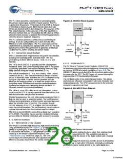
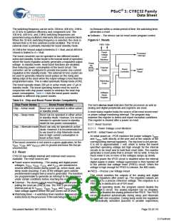
Figure 6-5. Power Mode Transitions
6.2.1.5 Wakeup Events
Wakeup events are configurable and can come from an interrupt
or device reset. A wakeup event restores the system to active
mode. Firmware enabled interrupt sources include internally
generated interrupts, power supervisor, central timewheel, and
I/O interrupts. Internal interrupt sources can come from a variety
of peripherals, such as analog comparators and UDBs. The
central timewheel provides periodic interrupts to allow the
system to wake up, poll peripherals, or perform real-time
functions. Reset event sources include the external reset I/O pin
(XRES), WDT, and Precision Reset (PRES).
Active
Manual
Sleep
Hibernate
Buzz
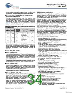
6.2.2 Boost Converter
Applications that use a supply voltage of less than 1.71 V, such
as solar or single cell battery supplies, may use the on-chip boost
converter. The boost converter may also be used in any system
that requires a higher operating voltage than the supply provides.
For instance, this includes driving 5.0 V LCD glass in a 3.3 V
system. The boost converter accepts an input voltage as low as
0.5 V. With one low cost inductor it produces a selectable output
voltage sourcing enough current to operate the PSoC and other
on-board components.
Alternate
Active
6.2.1.1 Active Mode
Active mode is the primary operating mode of the device. When
in active mode, the active configuration template bits control
which available resources are enabled or disabled. When a
resource is disabled, the digital clocks are gated, analog bias
currents are disabled, and leakage currents are reduced as
appropriate. User firmware can dynamically control subsystem
power by setting and clearing bits in the active configuration
template. The CPU can disable itself, in which case the CPU is
automatically reenabled at the next wakeup event.
The boost converter accepts an input voltage from 0.5 V to 5.5 V
(VBAT), and can start up with VBAT as low as 0.5 V. The converter
provides a user configurable output voltage of 1.8 to 5.0 V
(VBOOST). VBAT is typically less than VBOOST; if VBAT is greater
than or equal to VBOOST, then VBOOST will be the same as VBAT
The block can deliver up to 50 mA (IBOOST) depending on
configuration.
.
When a wakeup event occurs, the global mode is always
returned to active, and the CPU is automatically enabled,
regardless of its template settings. Active mode is the default
global power mode upon boot.
Four pins are associated with the boost converter: VBAT, VSSB
,
VBOOST, and Ind. The boosted output voltage is sensed at the
VBOOST pin and must be connected directly to the chip’s supply
inputs. An inductor is connected between the VBAT and Ind pins.
You can optimize the inductor value to increase the boost
converter efficiency based on input voltage, output voltage,
current and switching frequency. The External Schottky diode
shown in Figure 6-6 is required only in cases when
6.2.1.2 Alternate Active Mode
Alternate Active mode is very similar to Active mode. In alternate
active mode, fewer subsystems are enabled, to reduce power
consumption. One possible configuration is to turn off the CPU
and flash, and run peripherals at full speed.
VBOOST > 3.6 V.
6.2.1.3 Sleep Mode
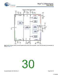
Figure 6-6. Application for Boost Converter
Sleep mode reduces power consumption when a resume time of
15 µs is acceptable. The wake time is used to ensure that the
regulator outputs are stable enough to directly enter active
mode.
Vdda Vddd Vddio
Vboost
Ind
Optional
Schottky Diode
Only required
Vboost>3.6 V
6.2.1.4 Hibernate Mode
In hibernate mode nearly all of the internal functions are
disabled. Internal voltages are reduced to the minimal level to
keep vital systems alive. Configuration state is preserved in
hibernate mode and SRAM memory is retained. GPIOs
configured as digital outputs maintain their previous values and
external GPIO pin interrupt settings are preserved. The device
can only return from hibernate mode in response to an external
I/O interrupt. The resume time from hibernate mode is less than
100 µs.
22 µF 0. 1 µF
PSoC
10µH
22 µF
SMP
Vbat
Vssb
Vssa
Vssd
Document Number: 001-56955 Rev. *J
Page 32 of 119
[+] Feedback

 CYPRESS [ CYPRESS ]