PSoC® 3: CY8C32 Family
Data Sheet
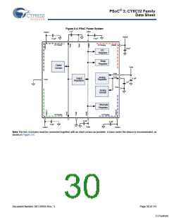
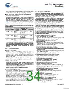
The switching frequency can be set to 100 kHz, 400 kHz, 2 MHz,
or 32 kHz to optimize efficiency and component cost. The
100 kHz, 400 kHz, and 2 MHz switching frequencies are
generated using oscillators internal to the boost converter block.
When the 32-kHz switching frequency is selected, the clock is
derived from a 32 kHz external crystal oscillator. The 32-kHz
external clock is primarily intended for boost standby mode.
by firmware within a certain period of time, the watchdog timer
generates a reset.
Software – The device can be reset under program control.
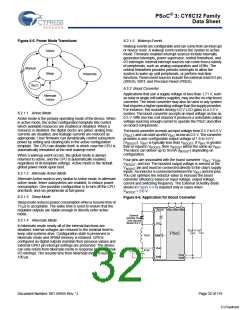
Figure 6-7. Resets
Vddd Vdda
At 2 MHz the Vboost output is limited to 2 × Vbat, and at 400 kHz
Vboost is limited to 4 × Vbat.
Power
Voltage
Level
Monitors
Processor
Interrupt
The boost converter can be operated in two different modes:
active and standby. Active mode is the normal mode of operation
where the boost regulator actively generates a regulated output
voltage. In standby mode, most boost functions are disabled,
thus reducing power consumption of the boost circuit. The
converter can be configured to provide low-power, low-current
regulation in the standby mode. The external 32 kHz crystal can
be used to generate inductor boost pulses on the rising and
falling edge of the clock when the output voltage is less than the
programmed value. This is called automatic thump mode (ATM).
Reset
Pin
External
Reset
Reset
Controller
System
Reset
Watchdog
Timer
The boost typically draws 200 µA in active mode and 12 µA in
standby mode. The boost operating modes must be used in
conjunction with chip power modes to minimize the total chip
power consumption. Table 6-4 lists the boost power modes
available in different chip power modes.
Software
Reset
Register
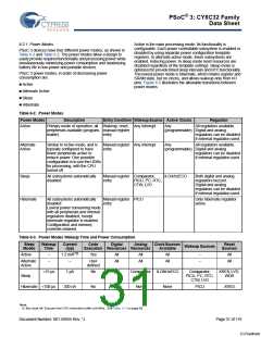
Table 6-4. Chip and Boost Power Modes Compatibility
Chip Power Modes
Boost Power Modes
The term device reset indicates that the processor as well as
analog and digital peripherals and registers are reset.
Chip – Active mode
Boost can be operated in either active
or standby mode.
A reset status register holds the source of the most recent reset
or power voltage monitoring interrupt. The program may
examine this register to detect and report exception conditions.
This register is cleared after a power-on reset.
Chip – Sleep mode
Boost can be operated in either active
or standby mode. However, it is recom-
mended to operate boost in standby
mode for low-power consumption
6.3.1 Reset Sources
Chip – Hibernate mode Boost can only be operated in active
mode. However, it is recommended not
to use boost in chip hibernate mode
due to high current consumption in
boost active mode
6.3.1.1 Power Voltage Level Monitors
IPOR – Initial Power-on Reset
At initial power-on, IPOR monitors the power voltages VDDD
and VDDA, both directly at the pins and at the outputs of the
corresponding internal regulators. The trip level is not precise.
It is set to approximately 1 volt, which is below the lowest
specified operating voltage but high enough for the internal
circuits to be reset and to hold their reset state. The monitor
generates a reset pulse that is at least 100 ns wide. It may be
much wider if one or more of the voltages ramps up slowly.
To save power the IPOR circuit is disabled when the internal
digital supply is stable. Voltage supervision is then handed off
to the precise low voltage reset (PRES) circuit. When the
voltage is high enough for PRES to release, the IMO starts.
If the boost converter is not used in a given application, tie the
VBAT, VSSB, and VBOOST pins to ground and leave the Ind pin
unconnected.
6.3 Reset
CY8C32 has multiple internal and external reset sources
available. The reset sources are:
Power source monitoring – The analog and digital power
voltages, VDDA, VDDD, VCCA, and VCCD are monitored in
several different modes during power up, active mode, and
sleep mode (buzzing). If any of the voltages goes outside
predetermined ranges then a reset is generated. The monitors
are programmable to generate an interrupt to the processor
under certain conditions before reaching the reset thresholds.
External – The device can be reset from an external source by
pulling the reset pin (XRES) low. The XRES pin includes an
internal pull-up to VDDIO1. VDDD, VDDA, and VDDIO1 must all
have voltage applied before the part comes out of reset.
PRES – Precise Low Voltage Reset
This circuit monitors the outputs of the analog and digital
internal regulators after power up. The regulator outputs are
compared to a precise reference voltage. The response to a
PRES trip is identical to an IPOR reset.
In normal operating mode, the program cannot disable the
digital PRES circuit. The analog regulator can be disabled,
which also disables the analog portion of the PRES. The PRES
circuit is disabled automatically during sleep and hibernate
modes, with one exception: During sleep mode the regulators
are periodically activated (buzzed) to provide supervisory
Watchdog timer – A watchdog timer monitors the execution of
instructions by the processor. If the watchdog timer is not reset
Document Number: 001-56955 Rev. *J
Page 33 of 119
[+] Feedback

 CYPRESS [ CYPRESS ]