PSoC® 3: CY8C32 Family
Data Sheet
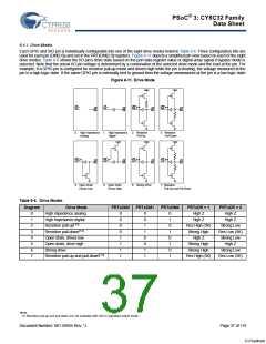
6.4.1 Drive Modes
Each GPIO and SIO pin is individually configurable into one of the eight drive modes listed in Table 6-6. Three configuration bits are
used for each pin (DM[2:0]) and set in the PRTxDM[2:0] registers. Figure 6-11 depicts a simplified pin view based on each of the eight
drive modes. Table 6-6 shows the I/O pin’s drive state based on the port data register value or digital array signal if bypass mode is
selected. Note that the actual I/O pin voltage is determined by a combination of the selected drive mode and the load at the pin. For
example, if a GPIO pin is configured for resistive pull-up mode and driven high while the pin is floating, the voltage measured at the
pin is a high logic state. If the same GPIO pin is externally tied to ground then the voltage unmeasured at the pin is a low logic state.
Figure 6-11. Drive Mode
Vddio
Vddio
DR
PS
DR
PS
DR
PS
DR
PS
Pin
Pin
Pin
Pin
0. High Impedance 1. High Impedance
Analog Digital
2. Resistive
Pull-Up
3. Resistive
Pull-Down
Vddio
Vddio
Vddio
DR
PS
DR
PS
DR
PS
DR
PS
Pin
Pin
Pin
Pin
4. Open Drain,
Drives Low
5. Open Drain,
Drives High
6. Strong Drive
7. Resistive
Pull-Up and Pull-Down
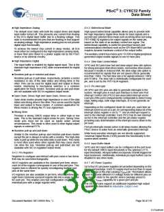
Table 6-6. Drive Modes
Diagram
Drive Mode
PRTxDM2
PRTxDM1
PRTxDM0
PRTxDR = 1
PRTxDR = 0
High Z
0
1
2
3
4
5
6
7
High impedence analog
High Impedance digital
Resistive pull-up[13]
Resistive pull-down[13]
Open drain, drives low
Open drain, drive high
Strong drive
0
0
0
0
1
1
1
1
0
0
1
1
0
0
1
1
0
1
0
1
0
1
0
1
High Z
High Z
High Z
Res High (5K)
Strong High
High Z
Strong Low
Res Low (5K)
Strong Low
High Z
Strong High
Strong High
Res High (5K)
Strong Low
Res Low (5K)
Resistive pull-up and pull-down[13]
Note
13. Resistive pull-up and pull-down are not available with SIO in regulated output mode.
Document Number: 001-56955 Rev. *J
Page 37 of 119
[+] Feedback

 CYPRESS [ CYPRESS ]