PSoC® 3: CY8C32 Family
Data Sheet
services and to reduce wakeup time. At these times the PRES
circuit is also buzzed to allow periodic voltage monitoring.
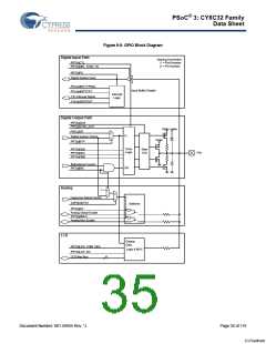
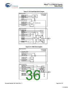
6.4 I/O System and Routing
PSoC I/Os are extremely flexible. Every GPIO has analog and
digital I/O capability. All I/Os have a large number of drive modes,
which are set at POR. PSoC also provides up to four individual
I/O voltage domains through the VDDIO pins.
ALVI, DLVI, AHVI – Analog/Digital Low Voltage Interrupt,
Analog High Voltage Interrupt
Interrupt circuits are available to detect when VDDA and VDDD
go outside a voltage range. For AHVI, VDDA is compared to a
fixed trip level. For ALVI and DLVI, VDDA and VDDD are
compared to trip levels that are programmable, as listed in
Table 6-5. ALVI and DLVI can also be configured to generate
a device reset instead of an interrupt.
There are two types of I/O pins on every device; those with USB
provide a third type. Both GPIO and Special I/O (SIO) provide
similar digital functionality. The primary differences are their
analog capability and drive strength. Devices that include USB
also provide two USBIO pins that support specific USB
functionality as well as limited GPIO capability.
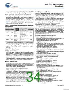
Table 6-5. Analog/Digital Low Voltage Interrupt, Analog High
Voltage Interrupt
All I/O pins are available for use as digital inputs and outputs for
both the CPU and digital peripherals. In addition, all I/O pins can
generate an interrupt. The flexible and advanced capabilities of
the PSoC I/O, combined with any signal to any pin routability,
greatly simplify circuit design and board layout. All GPIO pins can
be used for analog input, CapSense, and LCD segment drive,
while SIO pins are used for voltages in excess of VDDA and for
programmable output voltages.
Normal
Voltage
Range
Available Trip
Interrupt Supply
Accuracy
Settings
DLVI
ALVI
AHVI
VDDD 1.71 V –
5.5 V
1.70 V – 5.45 V
in 250 mV
increments
±2%
Features supported by both GPIO and SIO:
User programmable port reset state
SeparateI/OsuppliesandvoltagesforuptofourgroupsofI/O
Digital peripherals use DSI to connect the pins
Input or output or both for CPU and DMA
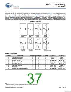
Eight drive modes
Every pin can be an interrupt source configured as rising
edge, falling edge or both edges. If required, level sensitive
interrupts are supported through the DSI
Dedicated port interrupt vector for each port
Slew rate controlled digital output drive mode
VDDA 1.71 V –
5.5 V
1.70 V – 5.45 V
in 250 mV
increments
±2%
±2%
VDDA 1.71 V –
5.5 V
5.75 V
The monitors are disabled until after IPOR. During sleep mode
these circuits are periodically activated (buzzed). If an interrupt
occurs during buzzing then the system first enters its wake up
sequence. The interrupt is then recognized and may be
serviced.
6.3.1.2 Other Reset Sources
Access port control and configuration registers on either port
basis or pin basis
XRES – External Reset
Separateportread(PS)andwrite(DR)dataregisterstoavoid
read modify write errors
Special functionality on a pin by pin basis
PSoC 3 has either a single GPIO pin that is configured as an
external reset or a dedicated XRES pin. Either the dedicated
XRES pin or the GPIO pin, if configured, holds the part in reset
while held active (low). The response to an XRES is the same
as to an IPOR reset.
Additional features only provided on the GPIO pins:
LCD segment drive on LCD equipped devices
CapSense
Analog input and output capability
Continuous 100 µA clamp current capability
Standard drive strength down to 1.7 V
The external reset is active low. It includes an internal pull-up
resistor. XRES is active during sleep and hibernate modes.
SRES – Software Reset
Additional features only provided on SIO pins:
Higher drive strength than GPIO
Hot swap capability (5 V tolerance at any operating VDD
Programmable and regulated high input and output drive
levels down to 1.2 V
A reset can be commanded under program control by setting
a bit in the software reset register. This is done either directly
by the program or indirectly by DMA access. The response to
a SRES is the same as after an IPOR reset.
)
Another register bit exists to disable this function.
No analog input, CapSense, or LCD capability
Over voltage tolerance up to 5.5 V
WRES – Watchdog Timer Reset
The watchdog reset detects when the software program is no
longer being executed correctly. To indicate to the watchdog
timer that it is running correctly, the program must periodically
reset the timer. If the timer is not reset before a user-specified
amount of time, then a reset is generated.
SIO can act as a general purpose analog comparator
USBIO features:
Full speed USB 2.0 compliant I/O
Highest drive strength for general purpose use
Input, output, or both for CPU and DMA
Input, output, or both for digital peripherals
Digital output (CMOS) drive mode
Note IPOR disables the watchdog function. The program must
enable the watchdog function at an appropriate point in the
code by setting a register bit. When this bit is set, it cannot be
cleared again except by an IPOR power-on reset event.
Each pin can be an interrupt source configured as rising
edge, falling edge, or both edges
Document Number: 001-56955 Rev. *J
Page 34 of 119
[+] Feedback

 CYPRESS [ CYPRESS ]