CY7C64013
CY7C64113
16.4
Timer Interrupt
There are two periodic timer interrupts: the 128-µs interrupt and the 1.024-ms interrupt. The user should disable both timer
interrupts before going into the suspend mode to avoid possible conflicts between servicing the timer interrupts first or the suspend
request first.
16.5
USB Endpoint Interrupts
There are five USB endpoint interrupts, one per endpoint. A USB endpoint interrupt is generated after the USB host writes to a
USB endpoint FIFO or after the USB controller sends a packet to the USB host. The interrupt is generated on the last packet of
the transaction (e.g., on the host’s ACK during an IN, or on the device ACK during on OUT). If no ACK is received during an IN
transaction, no interrupt is generated.
16.6
DAC Interrupt
Each DAC I/O pin can generate an interrupt, if enabled. The interrupt polarity for each DAC I/O pin is programmable. A positive
polarity is a rising edge input while a negative polarity is a falling edge input. All of the DAC pins share a single interrupt vector,
which means the firmware needs to read the DAC port to determine which pin or pins caused an interrupt.
If one DAC pin has triggered an interrupt, no other DAC pins can cause a DAC interrupt until that pin has returned to its inactive
(non-trigger) state or the corresponding interrupt enable bit is cleared. The USB Controller does not assign interrupt priority to
different DAC pins and the DAC Interrupt Enable Register is not cleared during the interrupt acknowledge process.
16.7
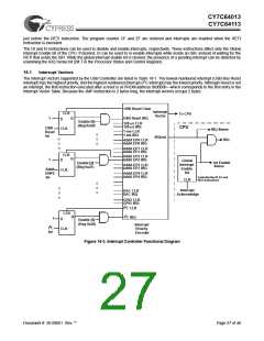
GPIO/HAPI Interrupt
Each of the GPIO pins can generate an interrupt, if enabled. The interrupt polarity can be programmed for each GPIO port as
part of the GPIO configuration. All of the GPIO pins share a single interrupt vector, which means the firmware needs to read the
GPIO ports with enabled interrupts to determine which pin or pins caused an interrupt. A block diagram of the GPIO interrupt
logic is shown in Figure 16-5. Refer to Sections 9.1 and 9.2 for more information of setting GPIO interrupt polarity and enabling
individual GPIO interrupts.
If one port pin has triggered an interrupt, no other port pins can cause a GPIO interrupt until that port pin has returned to its
inactive (non-trigger) state or its corresponding port interrupt enable bit is cleared. The USB Controller does not assign interrupt
priority to different port pins and the Port Interrupt Enable Registers are not cleared during the interrupt acknowledge process.
Port
Configuration
GPIO Interrupt
Flip Flop
Register
OR Gate
(1 input per
GPIO pin)
IRQout
Interrupt
Priority
1
D
Q
M
U
X
Interrupt
Vector
Encoder
GPIO
Pin
CLR
Port Interrupt
Enable Register
1 = Enable
0 = Disable
IRA
Global
GPIO Interrupt
Enable
1 = Enable
0 = Disable
(Bit 5, Register 0x20)
Figure 16-5. GPIO Interrupt Structure
When HAPI is enabled, the HAPI logic takes over the interrupt vector and blocks any interrupt from the GPIO bits, including
ports/bits not being used by HAPI. Operation of the HAPI interrupt is independent of the GPIO specific bit interrupt enables, and
is enabled or disabled only by bit 5 of the Global Interrupt Enable Register (0x20) when HAPI is enabled. The settings of the
GPIO bit interrupt enables on ports/bits not used by HAPI still effect the CMOS mode operation of those ports/bits. The effect of
Document #: 38-08001 Rev. **
Page 29 of 48

 CYPRESS [ CYPRESS ]