CY7C64013
CY7C64113
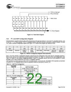
Table 14-1. Port 2 Pin and HAPI Configuration Bit Definitions
Pin
Name
LatEmptyPin
DReadyPin
STB
Direction
Description (Port 2 Pin)
Ready for more input data from external interface.
Output data ready for external interface.
Strobe signal for latching incoming data.
Output Enable, causes chip to output data.
Chip Select (Gates STB and OE).
P2[2]
P2[3]
P2[4]
P2[5]
P2[6]
Out
Out
In
OE
In
CS
In
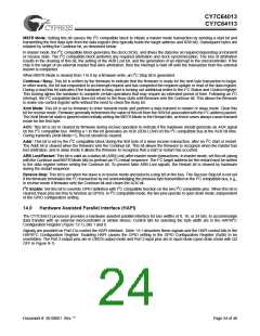
Bit
2
Name
R/W
R
Description (HAPI/I2C Configuration Register)
Asserted after firmware writes data to Port 0, until OE driven LOW.
Asserted after firmware reads data from Port 0, until STB driven LOW.
Data Ready
Latch Empty
DRDY Polarity
3
R
4
R/W
Determines polarity of Data Ready bit and DReadyPin:
If 0, Data Ready is active LOW, DReadyPin is active HIGH.
If 1, Data Ready is active HIGH, DReadyPin is active LOW.
5
LEMPTY Polarity
R/W
Determines polarity of Latch Empty bit and LatEmptyPin:
If 0, Latch Empty is active LOW, LatEmptyPin is active HIGH.
If 1, Latch Empty is active HIGH, LatEmptyPin is active LOW.
HAPI Read by External Device from CY7C64x13: In this case (see Figure 23-3), firmware writes data to the GPIO ports. If
16-bit or 24-bit transfers are being made, Port 0 should be written last, since writes to Port 0 asserts the Data Ready bit and the
DReadyPin to signal the external device that data is available.
The external device then drives the OE and CS pins active (LOW), which causes the HAPI data to be output on the port pins.
When OE is returned HIGH (inactive), the HAPI/GPIO interrupt is generated. At that point, firmware can reload the HAPI latches
for the next output, again writing Port 0 last.
The Data Ready bit reads the opposite state from the external DReadyPin on pin P2[3]. If the DRDY Polarity bit is 0, DReadyPin
is active HIGH, and the Data Ready bit is active LOW.
HAPI Write by External Device to CY7C64x13: In this case (see Figure 23-4), the external device drives the STB and CS pins
active (LOW) when it drives new data onto the port pins. When this happens, the internal latches become full which causes the
Latch Empty bit to be deasserted. When STB is returned HIGH (inactive), the HAPI/GPIO interrupt is generated. Firmware then
reads the parallel ports to empty the HAPI latches. If 16-bit or 24-bit transfers are being made, Port 0 should be read last because
reads from Port 0 assert the Latch Empty bit and the LatEmptyPin to signal the external device for more data.
The Latch Empty bit reads the opposite state from the external LatEmptyPin on pin P2[2]. If the LEMPTY Polarity bit is 0,
LatEmptyPin is active HIGH, and the Latch Empty bit is active LOW.
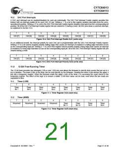
15.0
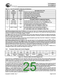
Processor Status and Control Register
7
R
6
5
4
3
2
1
0
R/W
R/W
R/W
R/W
R
R/W
Run
IRQ
Pending
Watch Dog
Reset
USB Bus Re-
set Interrupt
Power-On
Reset
Suspend
Interrupt
Enable Sense
reserved
Figure 15-1. Processor Status and Control Register 0xFF
The Run bit, bit 0, is manipulated by the HALT instruction. When Halt is executed, all the bits of the Processor Status and Control
Register are cleared to 0. Since the run bit is cleared, the processor stops at the end of the current instruction. The processor
remains halted until an appropriate reset occurs (power-on or watch dog). This bit should normally be written as a ‘1.’
Bit 1 is reserved and must be written as a zero.
The Interrupt Enable Sense (bit 2) shows whether interrupts are enabled or disabled. Firmware has no direct control over this bit
as writing a zero or one to this bit position has no effect on interrupts. A ‘0’ indicates that interrupts are masked off and a ‘1’
indicates that the interrupts are enabled. This bit is further gated with the bit settings of the Global Interrupt Enable Register (0x20)
and USB End Point Interrupt Enable Register (0x21). Instructions DI, EI, and RETI manipulate the state of this bit.
Writing a ‘1’ to the Suspend bit (bit 3) halts the processor and causes the microcontroller to enter the suspend mode that
significantly reduces power consumption. A pending, enabled interrupt or USB bus activity causes the device to come out of
suspend. After coming out of suspend, the device resumes firmware execution at the instruction following the IOWR which put
the part into suspend. An IOWR attempting to put the part into suspend is ignored if non-idle USB bus activity is present. See
Section 8.0 for more details on suspend mode operation.
Document #: 38-08001 Rev. **
Page 25 of 48

 CYPRESS [ CYPRESS ]