CY7C64013
CY7C64113
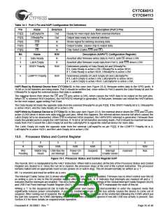
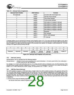
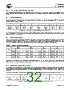
Table 16-1. Interrupt Vector Assignments
Interrupt Vector Number
ROM Address
0x0000
0x0002
0x0004
0x0006
0x0008
0x000A
0x000C
0x000E
0x0010
0x0012
0x0014
0x0016
0x0018
Function
Not Applicable
Execution after Reset begins here
USB Bus Reset interrupt
128-µs timer interrupt
1
2
3
1.024-ms timer interrupt
USB Address A Endpoint 0 interrupt
USB Address A Endpoint 1 interrupt
USB Address A Endpoint 2 interrupt
USB Address A Endpoint 3 interrupt
USB Address A Endpoint 4 interrupt
Reserved
4
5
6
7
8
9
10
11
12
DAC interrupt
GPIO / HAPI interrupt
I2C interrupt
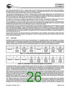
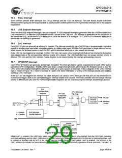
A pending address can be read from the Interrupt Vector Register (Figure 16-4). The value read from this register is only valid if
the Global Interrupt bit has been disabled, by executing the DI instruction or in an Interrupt Service Routine before interrupts have
been re-enabled. The value read from this register is the interrupt vector address; for example, a 0x06 indicates the 1 ms timer
interrupt is the highest priority pending interrupt.
7
6
5
4
3
2
1
0
R
R
R
R
R
Reserved
Reserved
Reserved
Interrupt
Vector Bit 4
Interrupt
Vector Bit 3
Interrupt
Vector Bit 2
Interrupt
Vector Bit 1
Reads ‘0’
Figure 16-4. Interrupt Vector Register 0x23 (read only)
16.2
Interrupt Latency
Interrupt latency can be calculated from the following equation:
Interrupt latency = (Number of clock cycles remaining in the current instruction) + (10 clock cycles for the CALL instruction) +
(5 clock cycles for the JMP instruction)
For example, if a 5 clock cycle instruction such as JC is being executed when an interrupt occurs, the first instruction of the
Interrupt Service Routine executes a minimum of 16 clocks (1+10+5) or a maximum of 20 clocks (5+10+5) after the interrupt is
issued. For a 12-MHz internal clock (6-MHz crystal), 20 clock periods is 20 / 12 MHz = 1.667 µs.
16.3
USB Bus Reset Interrupt
The USB Controller recognizes a USB Reset when a Single Ended Zero (SE0) condition persists on the upstream USB port for
12–16 µs (the Reset may be recognized for an SE0 as short as 12 µs, but is always recognized for an SE0 longer than 16 µs).
SE0 is defined as the condition in which both the D+ line and the D– line are LOW. Bit 5 of the Status and Control Register is set
to record this event. The interrupt is asserted at the end of the Bus Reset. If the USB reset occurs during the start-up delay
following a POR, the delay is aborted as described in Section 7.1. The USB Bus Reset Interrupt is generated when the SE0 state
is deasserted.
A USB Bus Reset clears the following registers:
SIE Section:USB Device Address Registers (0x10, 0x40)
Document #: 38-08001 Rev. **
Page 28 of 48

 CYPRESS [ CYPRESS ]