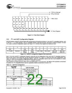
CY7C64013
CY7C64113
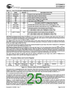
The Power-On Reset (bit 4) is set to ‘1’ during a power-on reset. The firmware can check bits 4 and 6 in the reset handler to
determine whether a reset was caused by a power-on condition or a watch dog timeout. Note that a POR event may be followed
by a watch dog reset before firmware begins executing, as explained below.
The USB Bus Reset Interrupt (bit 5) occurs when a USB Bus Reset is received on the upstream port. The USB Bus Reset is a
single-ended zero (SE0) that lasts from 12 to 16 µs. An SE0 is defined as the condition in which both the D+ line and the D– line
are LOW at the same time. When the SIE detects that this SE0 condition is removed, the USB Bus Reset interrupt bit is set in
the Processor Status and Control Register and a USB Bus Reset interrupt is generated.
The Watch Dog Reset (bit 6) is set during a reset initiated by the Watch Dog Timer. This indicates the Watch Dog Timer went for
more than tWATCH (8 ms minimum) between Watch Dog clears. This can occur with a POR event, as noted below.
The IRQ pending (bit 7), when set, indicates that one or more of the interrupts has been recognized as active. An interrupt remains
pending until its interrupt enable bit is set (registers 0x20 or 0x21) and interrupts are globally enabled. At that point, the internal
interrupt handling sequence clears this bit until another interrupt is detected as pending.
During power-up, the Processor Status and Control Register is set to 00010001, which indicates a POR (bit 4 set) has occurred
and no interrupts are pending (bit 7 clear). During the 96 ms suspend at start-up (explained in Section 7.1), a Watch Dog Reset
also occurs unless this suspend is aborted by an upstream SE0 before 8 ms. If a WDR occurs during the power-up suspend
interval, firmware reads 01010001 from the Status and Control Register after power-up. Normally, the POR bit should be cleared
so a subsequent WDR can be clearly identified. If an upstream bus reset is received before firmware examines this register, the
Bus Reset bit may also be set.
During a Watch Dog Reset, the Processor Status and Control Register is set to 01XX0001, which indicates a Watch Dog Reset
(bit 6 set) has occurred and no interrupts are pending (bit 7 clear). The Watch Dog Reset does not effect the state of the POR
and the Bus Reset Interrupt bits.
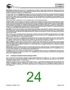
16.0
Interrupts
Interrupts are generated by the GPIO/DAC pins, the internal timers, I2C compatible interface or HAPI operation, or on various
USB traffic conditions. All interrupts are maskable by the Global Interrupt Enable Register and the USB End Point Interrupt Enable
Register. Writing a ‘1’ to a bit position enables the interrupt associated with that bit position. During a reset, the contents the Global
Interrupt Enable Register and USB End Point Interrupt Enable Register are cleared, effectively disabling all interrupts.
7
6
5
4
3
2
1
0
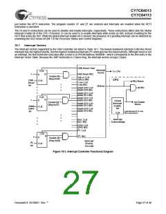
R/W
R/W
R/W
R/W
R/W
R/W
Reserved
I2C
Interrupt
Enable
GPIO/HAPI
Interrupt
Enable
DAC
Interrupt
Enable
Reserved
1.024-ms
Interrupt
Enable
128-µs
Interrupt
Enable
USB Bus RST
Interrupt
Enable
Figure 16-1. Global Interrupt Enable Register 0x20 (read/write)
7
6
5
4
3
2
1
0
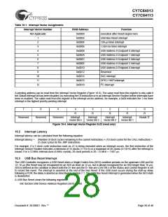
R/W
R/W
R/W
R/W
R/W
Reserved
Reserved
Reserved
EPB1
Interrupt
Enable
EPB0
Interrupt
Enable
EPA2
Interrupt
Enable
EPA1
Interrupt
Enable
EPA0
Interrupt
Enable
Figure 16-2. USB Endpoint Interrupt Enable Register 0x21 (read/write)
The interrupt controller contains a separate flip-flop for each interrupt. See Figure 16-3 for the logic block diagram of the interrupt
controller. When an interrupt is generated, it is first registered as a pending interrupt. It stays pending until it is serviced or a reset
occurs. A pending interrupt only generates an interrupt request if it is enabled by the corresponding bit in the interrupt enable
registers. The highest priority interrupt request is serviced following the completion of the currently executing instruction.
When servicing an interrupt, the hardware first disables all interrupts by clearing the Global Interrupt Enable bit in the CPU (the
state of this bit can be read at Bit 2 of the Processor Status and Control Register). Second, the flip-flop of the current interrupt is
cleared. This is followed by an automatic CALL instruction to the ROM address associated with the interrupt being serviced (i.e.,
the Interrupt Vector, see Section 16.1). The instruction in the interrupt table is typically a JMP instruction to the address of the
Interrupt Service Routine (ISR). The user can re-enable interrupts in the interrupt service routine by executing an EI instruction.
Interrupts can be nested to a level limited only by the available stack space.
The Program Counter value, as well as the Carry and Zero flags (CF, ZF), are stored onto the Program Stack by the automatic
CALL instruction generated as part of the interrupt acknowledge process. The user firmware is responsible for ensuring that the
processor state is preserved and restored during an interrupt. The PUSH A instruction should typically be used as the first
command in the ISR to save the accumulator value and the POP A instruction should be used to restore the accumulator value
Document #: 38-08001 Rev. **
Page 26 of 48

 CYPRESS [ CYPRESS ]