CY7C64013
CY7C64113
MSTR Mode: Setting this bit causes the I2C compatible block to initiate a master mode transaction by sending a start bit and
transmitting the first data byte from the data register (this typically holds the target address and R/W bit). Subsequent bytes are
initiated by setting the Continue bit, as described below.
In master mode, the I2C compatible block generates the clock (SCK), and drives the data line as required depending on transmit
or receive state. The I2C compatible block performs any required arbitration and clock synchronization. The loss of arbitration
results in the clearing of this bit, the setting of the ARB Lost bit, and the generation of an interrupt to the microcontroller. If the
chip is the target of an external master that wins arbitration, then the interrupt is held off until the transaction from the external
master is completed.
When MSTR Mode is cleared from 1 to 0 by a firmware write, an I2C Stop bit is generated.
Continue / Busy: This bit is written by the firmware to indicate that the firmware is ready for the next byte transaction to begin.
In other words, the bit has responded to an interrupt request and has completed the required update or read of the data register.
During a read this bit indicates if the hardware is busy and is locking out additional writes to the I2C Status and Control register.
This locking allows the hardware to complete certain operations that may require an extended period of time. Following an I2C
interrupt, the I2C compatible block does not return to the Busy state until firmware sets the Continue bit. This allows the firmware
to make one control register write without the need to check the Busy bit.
Xmit Mode: This bit is set by firmware to enter transmit mode and perform a data transmit in master or slave mode. Clear this
bit for receive mode. Firmware generally determines the value of this bit from the R/W bit associated with the I2C address packet.
The Xmit Mode bit state is ignored when initially writing the MSTR Mode or the Restart bits, as these cases always cause transmit
mode for the first byte.
ACK: This bit is set or cleared by firmware during receive operation to indicate if the hardware should generate an ACK signal
on the I2C compatible bus. Writing a 1 to this bit generates an ACK (SDA LOW) on the I2C compatible bus at the ACK bit time.
During transmits (Xmit Mode=1), this bit should be cleared.
Addr: This bit is set by the I2C compatible block during the first byte of a slave receive transaction, after an I2C start or restart.
The Addr bit is cleared when the firmware sets the Continue bit. This bit allows the firmware to recognize when the master has
lost arbitration, and in slave mode it allows the firmware to recognize that a start or restart has occurred.
ARB Lost/Restart: This bit is valid as a status bit (ARB Lost) after master mode transactions. In master mode, set this bit (along
with the Continue and MSTR Mode bits) to perform an I2C restart sequence. The I2C target address for the restart must be written
to the data register before setting the Continue bit. To prevent false ARB Lost signals, the Restart bit is cleared by hardware
during the restart sequence.
Receive Stop: This bit is set when the slave is in receive mode and detects a stop bit on the bus. The Receive Stop bit is not set
if the firmware terminates the I2C transaction by not acknowledging the previous byte transmitted on the I2C compatible bus, e.g.,
in receive mode if firmware sets the Continue bit and clears the ACK bit.
I2C Enable: Set this bit to override GPIO definition with I2C compatible function on the two I2C compatible pins. When this bit is
cleared, these pins are free to function as GPIOs. In I2C compatible mode, the two pins operate in open drain mode, independent
of the GPIO configuration setting.
14.0
Hardware Assisted Parallel Interface (HAPI)
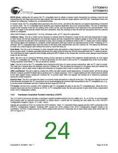
The CY7C64x13 processor provides a hardware assisted parallel interface for bus widths of 8, 16, or 24 bits, to accommodate
data transfer with an external microcontroller or similar device. Control bits for selecting the byte width are in the HAPI/I2C
Configuration Register (Figure 12-1), bits 1 and 0.
Signals are provided on Port 2 to control the HAPI interface. Table 14-1 describes these signals and the HAPI control bits in the
HAPI/I2C Configuration Register. Enabling HAPI causes the GPIO setting in the GPIO Configuration Register (0x08) to be
overridden. The Port 2 output pins are in CMOS output mode and Port 2 input pins are in input mode (open drain mode with Q3
OFF in Figure 9-1).
Document #: 38-08001 Rev. **
Page 24 of 48

 CYPRESS [ CYPRESS ]