CY7C64013
CY7C64113
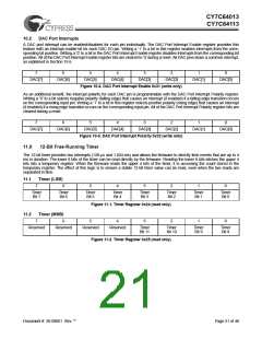
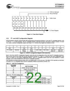
1.024-ms Interrupt
128-µs Interrupt
11 10
9
8
7
6
5
4
3
2
1
0
1-MHz Clock
L3 L2 L1 L0
D3 D2 D1 D0 D7 D6 D5 D4 D3 D2 D1 D0
To Timer Register
8
Figure 11-3. Timer Block Diagram
2
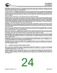
12.0
I C and HAPI Configuration Register
Internal hardware supports communication with external devices through two interfaces: a two-wire I2C compatible interface, and
a HAPI for 1, 2, or 3 byte transfers. The I2C compatible interface and HAPI functions, discussed in detail in Sections 13.0 and
14.0, share a common configuration register (see Figure 12-1). All bits of this register are cleared on reset.
7
6
5
4
3
R
2
R
1
0
R/W
R/W
R/W
R/W
R/W
I2C Position
Reserved
LEMPTY
Polarity
DRDY
Polarity
Latch Empty
Data Ready
HAPI Port
Width Bit 1
HAPI Port
Width Bit 0
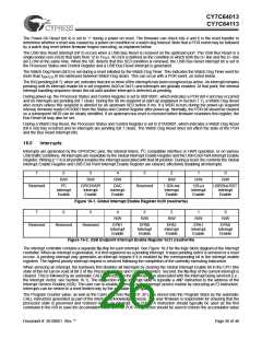
Figure 12-1. HAPI/I2C Configuration Register 0x09 (read/write)
Bits [7,1:0] of the HAPI/I2C Configuration Register control the pin out configuration of the HAPI and I2C compatible interfaces.
Bits [5:2] are used in HAPI mode only, and are described in Section 14.0. Table 12-1 shows the HAPI port configurations, and
Table 12-2 shows I2C pin location configuration options. These I2C compatible options exist due to pin limitations in certain
packages, and to allow simultaneous HAPI and I2C compatible operation.
HAPI operation is enabled whenever either HAPI Port Width Bit (Bit 1 or 0) is non-zero. This affects GPIO operation as described
in Section 14.0. I2C compatible blocks must be separately enabled as described in Section 13.0.
Table 12-1. HAPI Port Configuration
Port Width
Bits[1:0]
HAPI Port Width
24 Bits: P3[7:0], P1[7:0], P0[7:0]
16 Bits: P1[7:0], P0[7:0]
8 Bits: P0[7:0]
11
10
01
00
No HAPI Interface
Table 12-2. I2C Port Configuration
I2C Position
Bit[7]
Port Width
Bit[1]
I2C Position
X
0
1
1
0
0
I2C on P2[1:0], 0:SCL, 1:SDA
I2C on P1[1:0], 0:SCL, 1:SDA
I2C on P2[1:0], 0:SCL, 1:SDA
Document #: 38-08001 Rev. **
Page 22 of 48

 CYPRESS [ CYPRESS ]