CY7C64013
CY7C64113
2
13.0
I C Compatible Controller
The I2C compatible block provides a versatile two-wire communication with external devices, supporting master, slave, and
multi-master modes of operation. The I2C compatible block functions by handling the low-level signaling in hardware, and issuing
interrupts as needed to allow firmware to take appropriate action during transactions. While waiting for firmware response, the
hardware keeps the I2C compatible bus idle if necessary.
The I2C compatible block generates an interrupt to the microcontroller at the end of each received or transmitted byte, when a
stop bit is detected by the slave when in receive mode, or when arbitration is lost. Details of the interrupt responses are given in
Section 16.8.
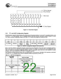
The I2C compatible interface consists of two registers, an I2C Data Register (Figure 13-1) and an I2C Status and Control Register
(Figure 13-2). The Data Register is implemented as separate read and write registers. Generally, the I2C Status and Control
Register should only be monitored after the I2C interrupt, as all bits are valid at that time. Polling this register at other times could
read misleading bit status if a transaction is underway.
The I2C SCL clock is connected to bit 0 of GPIO port 1 or GPIO port 2, and the I2C SDA data is connected to bit 1 of GPIO port
1 or GPIO port 2. Refer to Section 12.0 for the bit definitions and functionality of the HAPI/I2C Configuration Register, which is
used to set the locations of the configurable I2C compatible pins. Once the I2C compatible functionality is enabled by setting bit
0 of the I2C Status & Control Register, the two LSB bits ([1:0]) of the corresponding GPIO port are placed in Open Drain mode,
regardless of the settings of the GPIO Configuration Register.The electrical characteristics of the I2C compatible interface is the
same as that of GPIO ports 1 and 2. Note that the IOL (max) is 2 mA @ VOL = 2.0 V for ports 1 and 2.
All control of the I2C clock and data lines is performed by the I2C compatible block.
7
6
5
4
3
2
1
0
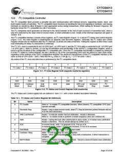
I2C Data 7
I2C Data 6
I2C Data 5
I2C Data 4
I2C Data 3
I2C Data 2
I2C Data 1
I2C Data 0
Figure 13-1. I2C Data Register 0x29 (separate read/write registers)
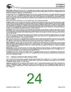
7
6
5
4
3
2
1
0
R/W
R/W
R/W
R/W
ACK
R/W
Addr
R/W
R/W
R/W
I2C
MSTR
Mode
Continue/
Busy
Xmit
Mode
ARB Lost/
Restart
Received
Stop
Enable
Figure 13-2. I2C Status and Control Register 0x28 (read/write)
The I2C Status and Control register bits are defined in Table 13-1, with a more detailed description following.
Table 13-1. I2C Status and Control Register Bit Definitions
Bit
Name
I2C Enable
Description
0
Write to 1 to enable I2C compatible function. When cleared, I2C compatible GPIO pins
operate normally.
1
2
3
4
Received Stop
ARB Lost/Restart
Addr
Reads 1 only in slave receive mode, when I2C Stop bit detected (unless firmware did not
ACK the last transaction).
Reads 1 to indicate master has lost arbitration. Reads 0 otherwise.
Write to 1 in master mode to perform a restart sequence (also set Continue bit).
Reads 1 during first byte after start/restart in slave mode, or if master loses arbitration.
Reads 0 otherwise. This bit should always be written as 0.
ACK
In receive mode, write 1 to generate ACK, 0 for no ACK.
In transmit mode, reads 1 if ACK was received, 0 if no ACK received.
5
6
Xmit Mode
Write to 1 for transmit mode, 0 for receive mode.
Continue / Busy
Write 1 to indicate ready for next transaction.
Reads 1 when I2C compatible block is busy with a transaction, 0 when transaction is
complete.
7
MSTR Mode
Write to 1 for master mode, 0 for slave mode. This bit is cleared if master loses arbitration.
Clearing from 1 to 0 generates Stop bit.
Document #: 38-08001 Rev. **
Page 23 of 48

 CYPRESS [ CYPRESS ]