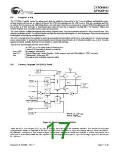
CY7C64013
CY7C64113
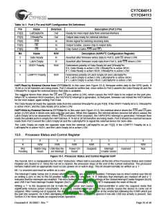
10.2
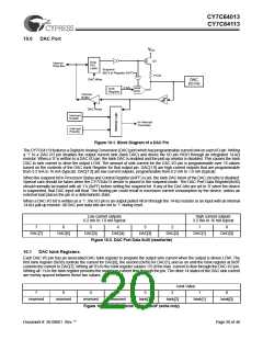
DAC Port Interrupts
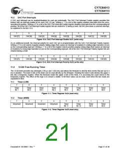
A DAC port interrupt can be enabled/disabled for each pin individually. The DAC Port Interrupt Enable register provides this
feature with an interrupt enable bit for each DAC I/O pin. Writing a ‘1’ to a bit in this register enables interrupts from the corre-
sponding bit position. Writing a ‘0’ to a bit in the DAC Port Interrupt Enable register disables interrupts from the corresponding bit
position. All of the DAC Port Interrupt Enable register bits are cleared to ‘0’ during a reset. All DAC pins share a common interrupt,
as explained in Section 16.6.
7
6
5
4
3
2
1
0
DAC[7]
DAC[6]
DAC[5]
DAC[4]
DAC[3]
DAC[2]
DAC[1]
DAC[0]
Figure 10-4. DAC Port Interrupt Enable 0x31 (write only)
As an additional benefit, the interrupt polarity for each DAC pin is programmable with the DAC Port Interrupt Polarity register.
Writing a ‘0’ to a bit selects negative polarity (falling edge) that causes an interrupt (if enabled) if a falling edge transition occurs
on the corresponding input pin. Writing a ‘1’ to a bit in this register selects positive polarity (rising edge) that causes an interrupt
(if enabled) if a rising edge transition occurs on the corresponding input pin. All of the DAC Port Interrupt Polarity register bits are
cleared during a reset.
7
6
5
4
3
2
1
0
DAC[7]
DAC[6]
DAC[5]
DAC[4]
DAC[3]
DAC[2]
DAC[1]
DAC[0]
Figure 10-5. DAC Port Interrupt Polarity 0x32 (write only)
11.0
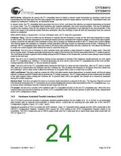
12-Bit Free-Running Timer
The 12-bit timer provides two interrupts (128-µs and 1.024-ms) and allows the firmware to directly time events that are up to 4
ms in duration. The lower 8 bits of the timer can be read directly by the firmware. Reading the lower 8 bits latches the upper 4
bits into a temporary register. When the firmware reads the upper 4 bits of the timer, it is accessing the count stored in the
temporary register. The effect of this logic is to ensure a stable 12-bit timer value can be read, even when the two reads are
separated in time.
11.1
Timer (LSB)
7
6
5
4
3
2
1
0
Timer
Bit 7
Timer
Bit 6
Timer
Bit 5
Timer
Bit 4
Timer
Bit 3
Timer
Bit 2
Timer
Bit 1
Timer
Bit 0
Figure 11-1. Timer Register 0x24 (read only)
11.2
Timer (MSB)
7
6
5
4
3
2
1
0
Reserved
Reserved
Reserved
Reserved
Timer
Bit 11
Timer
Bit 10
Timer
Bit 9
Timer
Bit 8
Figure 11-2. Timer Register 0x25 (read only)
Document #: 38-08001 Rev. **
Page 21 of 48

 CYPRESS [ CYPRESS ]