CY7C64013
CY7C64113
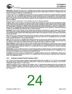
10.0
DAC Port
VCC
Q1
Data
Out
Latch
Internal
Data Bus
Suspend
(Bit 3 of Register 0xFF)
14 kΩ
DAC Write
DAC
I/O Pin
4 bits
Isink
Register
Isink
DAC
Internal
Buffer
DAC Read
Interrupt
Enable
to Interrupt
Controller
Interrupt
Polarity
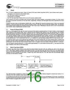
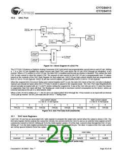
Figure 10-1. Block Diagram of a DAC Pin
The CY7C64113 features a Digital to Analog Conversion (DAC) port which has programmable current sink on each I/O pin. Writing
a ‘1’ to a DAC I/O pin disables the output current sink (Isink DAC) and drives the I/O pin HIGH through an integrated 14-kΩ
resistor. When a ‘0’ is written to a DAC I/O pin, the Isink DAC is enabled and the pull-up resistor is disabled. This causes the Isink
DAC to sink current to drive the output LOW. The amount of sink current for the DAC I/O pin is programmable over 16 values
based on the contents of the DAC Isink Register for that output pin. DAC[1:0] are high-current outputs that are programmable
from 3.2 mA to 16 mA (typical). DAC[7:2] are low-current outputs, programmable from 0.2 mA to 1.0 mA (typical).
When the suspend bit in Processor Status and Control Register (0xFF) is set, the Isink DAC block of the DAC circuitry is disabled.
Special care should be taken when the CY7C64x13 device is placed in the suspend mode. The DAC Port Data Register(0x30)
should normally be loaded with all ‘1’s (0xFF) before setting the suspend bit. If any of the DAC bits are set to ‘0’ when the device
is suspended, that DAC input will float. The floating pin could result in excessive current consumption by the device, unless an
external load places the pin in a deterministic state.
When a DAC I/O bit is written as a ‘1’, the I/O pin is an output pulled HIGH through the 14-kΩ resistor or an input with an internal
14-kΩ pull-up resistor. All DAC port data bits are set to ‘1’ during reset.
Low current outputs
0.2 mA to 1.0 mA typical
High current outputs
3.2 mA to 16 mA typical
7
6
5
4
3
2
1
0
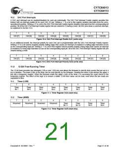
DAC[7]
DAC[6]
DAC[5]
DAC[4]
DAC[3]
DAC[2]
DAC[1]
DAC[0]
Figure 10-2. DAC Port Data 0x30 (read/write)
10.1
DAC Isink Registers
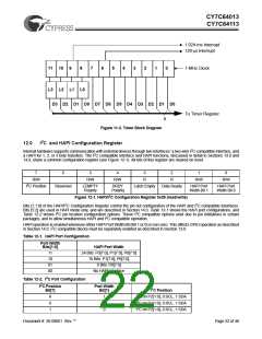
Each DAC I/O pin has an associated DAC Isink register to program the output sink current when the output is driven LOW. The
first Isink register (0x38) controls the current for DAC[0], the second (0x39) for DAC[1], and so on until the Isink register at 0x3F
controls the current to DAC[7]. Writing all ‘0’s to the Isink register causes 1/5 of the max. current to flow through the DAC I/O pin.
Writing all ‘1’s to the Isink register provides the maximum current flow through the pin. The other 14 states of the DAC sink current
are evenly spaced between these two values.
Isink Value
7
6
5
4
3
2
1
0
reserved
reserved
reserved
reserved
Isink[3]
Isink[2]
Isink[1]
Isink[0]
Figure 10-3. DAC Port Isink 0x38 to 0x3F (write only)
Document #: 38-08001 Rev. **
Page 20 of 48

 CYPRESS [ CYPRESS ]