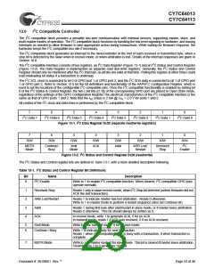
CY7C64013
CY7C64113
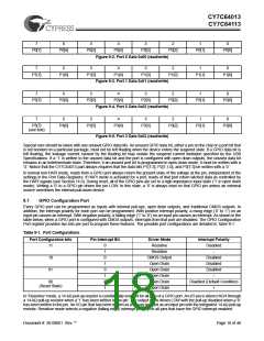
In “CMOS” mode, all pins of the GPIO port are outputs that are actively driven. A CMOS port is not a possible source for interrupts.
In “Open Drain” mode, the internal pull-up resistor and CMOS driver (HIGH) are both disabled. An open drain I/O pin that has
been written as a ‘1’ can be used as an input or an open drain output. An I/O pin that has been written as a ‘0’ drives the output
low. The interrupt polarity for an open drain GPIO port can be selected as positive (rising edge) or negative (falling edge).
During reset, all of the bits in the GPIO Configuration Register are written with ‘0’ to select Open Drain output for all GPIO ports
as the default configuration.
7
6
5
4
3
2
1
0
Port 3
Config Bit 1
Port 3
Config Bit 0
Port 2
Config Bit 1
Port 2
Config Bit 0
Port 1
Config Bit 1
Port 1
Config Bit 0
Port 0
Config Bit 1
Port 0
Config Bit 0
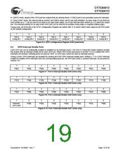
Figure 9-6. GPIO Configuration Register 0x08 (read/write)
9.2
GPIO Interrupt Enable Ports
Each GPIO pin can be individually enabled or disabled as an interrupt source. The Port 0–3 Interrupt Enable registers provide
this feature with an interrupt enable bit for each GPIO pin. When HAPI mode (discussed in Section 14.0) is enabled the GPIO
interrupts are blocked, including ports not used by HAPI, so GPIO pins cannot be used as interrupt sources.
During a reset, GPIO interrupts are disabled by clearing all of the GPIO interrupt enable ports. Writing a ‘1’ to a GPIO Interrupt
Enable bit enables GPIO interrupts from the corresponding input pin. All GPIO pins share a common interrupt, as discussed in
Section 16.7.
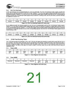
7
6
5
4
3
2
1
0
P0[7]
P0[6]
P0[5]
P0[4]
P0[3]
P0[2]
P0[1]
P0[0]
Figure 9-7. Port 0 Interrupt Enable 0x04 (write only)
7
6
5
4
3
2
1
0
P1[7]
P1[6]
P1[5]
P1[4]
P1[3]
P1[2]
P1[1]
P1[0]
Figure 9-8. Port 1 Interrupt Enable 0x05 (write only)
7
6
5
4
3
2
1
0
P2[7]
P2[6]
P2[5]
P2[4]
P2[3]
P2[2]
P2[1]
P2[0]
Figure 9-9. Port 2 Interrupt Enable 0x06 (write only)
7
6
5
4
3
2
1
0
reserved -
set to zero
P3[6]
P3[5]
P3[4]
P3[3]
P3[2]
P3[1]
P3[0]
Figure 9-10. Port 3 Interrupt Enable 0x07 (write only)
Document #: 38-08001 Rev. **
Page 19 of 48

 CYPRESS [ CYPRESS ]