CY7C64013
CY7C64113
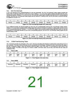
8.0
Suspend Mode
The CY7C64x13 can be placed into a low-power state by setting the Suspend bit of the Processor Status and Control register.
All logic blocks in the device are turned off except the GPIO interrupt logic and the USB receiver. The clock oscillator and PLL,
as well as the free-running and Watch Dog timers, are shut down. Only the occurrence of an enabled GPIO interrupt or non-idle
bus activity at a USB upstream or downstream port wakes the part out of suspend. The Run bit in the Processor Status and
Control Register must be set to resume a part out of suspend.
The clock oscillator restarts immediately after exiting suspend mode. The microcontroller returns to a fully functional state 1 ms
after the oscillator is stable. The microcontroller executes the instruction following the I/O write that placed the device into suspend
mode before servicing any interrupt requests.
The GPIO interrupt allows the controller to wake-up periodically and poll system components while maintaining a very low average
power consumption. To achieve the lowest possible current during suspend mode, all I/O should be held at VCC or Gnd. This also
applies to internal port pins that may not be bonded in a particular package.
Typical code for entering suspend is shown below:
...
...
; All GPIO set to low-power state (no floating pins)
; Enable GPIO interrupts if desired for wake-up
; Set suspend and run bits
; Write to Status and Control Register - Enter suspend, wait for USB activity (or GPIO Interrupt)
; This executes before any ISR
mov a, 09h
iowr FFh
nop
...
; Remaining code for exiting suspend routine
9.0
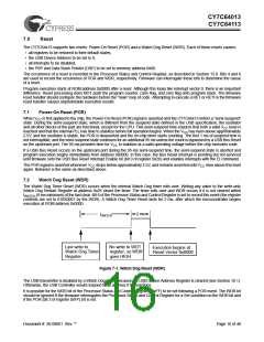
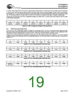
General-Purpose I/O (GPIO) Ports
VCC
GPIO
CFG
mode
2-bits
OE
Q2
Q1
Data
Out
Latch
Internal
Data Bus
14 kΩ
GPIO
PIN
Port Write
Port Read
Q3*
Data
In
Latch
Reg_Bit
STRB
(Latch is Transparent
except in HAPI mode)
Data
Interrupt
Latch
Interrupt
Enable
Interrupt
Controller
*Port 0,1,2: Low Isink
Port 3: High Isink
Figure 9-1. Block Diagram of a GPIO Pin
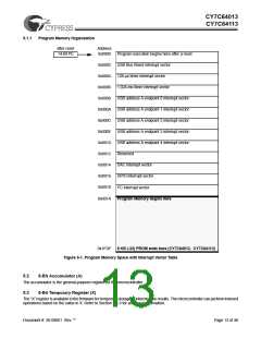
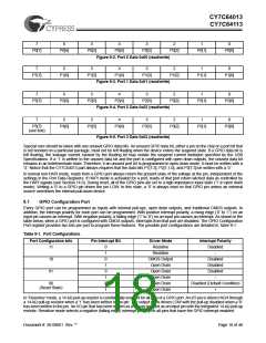
There are up to 32 GPIO pins (P0[7:0], P1[7:0], P2[7:0], and P3[7:0]) for the hardware interface. The number of GPIO pins
changes based on the package type of the chip. Each port can be configured as inputs with internal pull-ups, open drain outputs,
or traditional CMOS outputs. Port 3 offers a higher current drive, with typical current sink capability of 12 mA. The data for each
GPIO port is accessible through the data registers. Port data registers are shown in Figure 9-2 through Figure 9-5, and are set
to 1 on reset.
Document #: 38-08001 Rev. **
Page 17 of 48

 CYPRESS [ CYPRESS ]