CY7C64013
CY7C64113
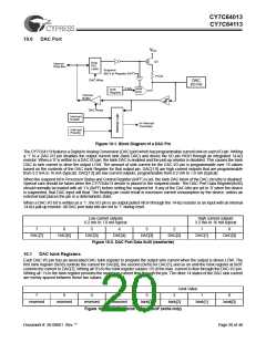
7.0
Reset
The CY7C64x13 supports two resets: Power-On Reset (POR) and a Watch Dog Reset (WDR). Each of these resets causes:
• all registers to be restored to their default states,
• the USB Device Address to be set to 0,
• all interrupts to be disabled,
• the PSP and Data Stack Pointer (DSP) to be set to memory address 0x00.
The occurrence of a reset is recorded in the Processor Status and Control Register, as described in Section 15.0. Bits 4 and 6
are used to record the occurrence of POR and WDR, respectively. Firmware can interrogate these bits to determine the cause
of a reset.
Program execution starts at ROM address 0x0000 after a reset. Although this looks like interrupt vector 0, there is an important
difference. Reset processing does NOT push the program counter, carry flag, and zero flag onto program stack. The firmware
reset handler should configure the hardware before the “main” loop of code. Attempting to execute a RET or RETI in the firmware
reset handler causes unpredictable execution results.
7.1
Power-On Reset (POR)
When VCC is first applied to the chip, the Power-On Reset (POR) signal is asserted and the CY7C64x13 enters a “semi-suspend”
state. During the semi-suspend state, which is different from the suspend state defined in the USB specification, the oscillator
and all other blocks of the part are functional, except for the CPU. This semi-suspend time ensures that both a valid VCC level is
reached and that the internal PLL has time to stabilize before full operation begins. When the VCC has risen above approximately
2.5V, and the oscillator is stable, the POR is deasserted and the on-chip timer starts counting. The first 1 ms of suspend time is
not interruptible, and the semi-suspend state continues for an additional 95 ms unless the count is bypassed by a USB Bus Reset
on the upstream port. The 95 ms provides time for VCC to stabilize at a valid operating voltage before the chip executes code.
If a USB Bus Reset occurs on the upstream port during the 95-ms semi-suspend time, the semi-suspend state is aborted and
program execution begins immediately from address 0x0000. In this case, the Bus Reset interrupt is pending but not serviced
until firmware sets the USB Bus Reset Interrupt Enable bit (bit 0 of register 0x20) and enables interrupts with the EI command.
The POR signal is asserted whenever VCC drops below approximately 2.5V, and remains asserted until VCC rises above this level
again. Behavior is the same as described above.
7.2
Watch Dog Reset (WDR)
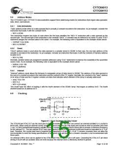
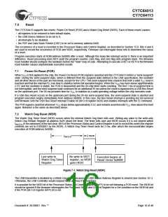
The Watch Dog Timer Reset (WDR) occurs when the internal Watch Dog timer rolls over. Writing any value to the write-only
Watch Dog Restart Register at address 0x26 clears the timer. The timer rolls over and WDR occurs if it is not cleared within
tWATCH (8 ms minimum) of the last clear. Bit 6 of the Processor Status and Control Register is set to record this event (the register
contents are set to 010X0001 by the WDR). A Watch Dog Timer Reset lasts for 2 ms, after which the microcontroller begins
execution at ROM address 0x0000.
2 ms
tWATCH
Last write to
Watch Dog Timer
Register
No write to WDT
register, so WDR
goes HIGH
Execution begins at
Reset Vector 0x0000
Figure 7-1. Watch Dog Reset (WDR)
The USB transmitter is disabled by a Watch Dog Reset because the USB Device Address Register is cleared (see Section 18.1).
Otherwise, the USB Controller would respond to all address 0 transactions.
It is possible for the WDR bit of the Processor Status and Control Register (0xFF) to be set following a POR event. The WDR bit
should be ignored If the firmware interrogates the Processor Status and Control Register for a Set condition on the WDR bit and
if the POR (bit 3 of register 0xFF) bit is set.
Document #: 38-08001 Rev. **
Page 16 of 48

 CYPRESS [ CYPRESS ]