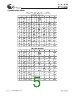
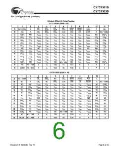
CY7C1361B
CY7C1363B
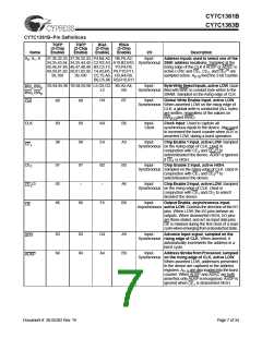
CY7C1361B–Pin Definitions (continued)
TQFP
(3-Chip
Enable)
TQFP
(2-Chip
Enable)
BGA
fBGA
(3-Chip
Enable)
(2-Chip
Enable)
Name
VSS
I/O
Ground
Description
Ground for the core of the device.
17,40,67,90 17,40,67,90 H2,D3,E3, C4,C5,C6,
F3,H3,K3, C7,C8,D5,
M3,N3,
D6,D7,E5,
P3,D5,E5, E6,E7,F5,
F5,H5,K5, F6,F7,G5,
M5,N5,P5 G6,G7,H5,
H6,H7,J5,
J6,J7,K5,K6,
K7,L5,L6,L7,
M5,M6,M7,
N4,N8
VSSQ
TDO
5,10,21,26, 5,10,21,26,
55,60,71,76 55,60,71,76
–
–
I/O Ground Ground for the I/O circuitry.
–
–
U5
P7
JTAG serial Serial data-out to the JTAG circuit.
output
Delivers data on the negative edge of TCK.
Synchronous If the JTAG feature is not being utilized, this
pin should be left unconnected. This pin is
not available on TQFP packages.
TDI
–
–
U3
P5
JTAG serial Serial data-In to the JTAG circuit. Sampled
input
ontherisingedgeofTCK. IftheJTAGfeature
Synchronous is not being utilized, this pin can be left
floating or connected to VDD through a pull
up resistor. This pin is not available on TQFP
packages.
TMS
–
–
–
–
U2
U4
R5
R7
JTAG serial Serial data-In to the JTAG circuit. Sampled
input
ontherisingedgeofTCK. IftheJTAGfeature
Synchronous is not being utilized, this pin can be discon-
nected or connected to VDD. This pin is not
available on TQFP packages.
TCK
NC
JTAG-
Clock input to the JTAG circuitry. If the
JTAG feature is not being utilized, this pin
must be connected to VSS. This pin is not
available on TQFP packages.
Clock
16,38,39,42, 16,38,39,42, B1,C1,R1, A1,A11,B1,
–
No Connects. Not internally connected to
the die. 18M, 36M, 72M, 144M and 288M are
address expansion pins are not internally
connected to the die.
66
14
43,66
14
T1,T2,J3, B11,C2,C10,
D4,L4,J5, H1,H3,H9,
R5,T6,U6, H10,N2,N5,
B7,C7,R7 N6,N7,N10,
P1,P2,R2
VSS/DNU
-
-
Ground/DNU This pin can be connected to Ground or
should be left floating.
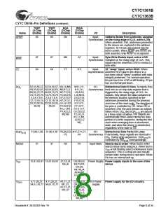
CY7C1363B: Pin Definitions
TQFP
(3-Chip
Enable)
TQFP
(2-Chip
Enable)
BGA
fBGA
(3-Chip
Enable)
(2-Chip
Enable)
Name
I/O
Description
A0, A1, A 37,36,32,33, 37,36,32,33, P4,N4,A2, R6,P6,A2,
Input-
Address Inputs used to select one of the
34,35,43,44, 34,35,44,45, C2,R2,T2, A10,A11,B2, Synchronous 512K address locations. Sampled at the
45,46,47,48, 46,47,48,49, A3,B3,C3, B10,P3,P4,
49,50,80,81, 50,80,81,82, T3,A5,B5, P8,P9,P10,
rising edge of the CLK if ADSP or ADSC is
active LOW, and CE1, CE2, and CE3[2] are
sampled active. A[1:0] feed the 2-bit counter.
82,99,100
92,99,100 C5,T5,A6, P11,R3,R4,
B6,C6,R6, R8,R9,R10,
T6
R11
Document #: 38-05302 Rev. *B
Page 9 of 34

 CYPRESS [ CYPRESS ]