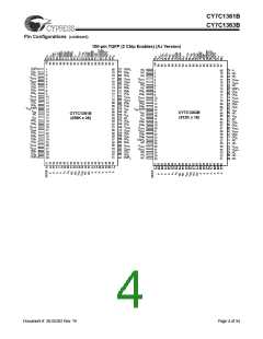
CY7C1361B
CY7C1363B
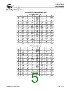
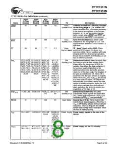
CY7C1361B–Pin Definitions (continued)
TQFP
(3-Chip
Enable)
TQFP
(2-Chip
Enable)
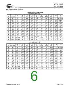
BGA
fBGA
(3-Chip
Enable)
(2-Chip
Enable)
Name
ADSC
I/O
Input-
Description
Address Strobe from Controller, sampled
85
85
B4
A8
Synchronous on the rising edge of CLK, active LOW.
When asserted LOW, addresses presented
to the device are captured in the address
registers. A[1:0] are also loaded into the
burst counter. When ADSP and ADSC are
both asserted, only ADSP is recognized.
87
64
87
64
M4
T7
A7
Input-
Byte Write Enable Input, active LOW.
BWE
ZZ
Synchronous Sampled on the rising edge of CLK. This
signal must be asserted LOW to conduct a
byte write.
H11
Input-
ZZ “sleep” Input, active HIGH. When
Asynchronous asserted HIGH places the device in a
non-time-critical “sleep” condition with data
integrity preserved. For normal operation,
this pin has to be LOW or left floating. ZZ pin
has an internal pull-down.
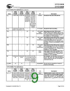
52,53,56,57, 52,53,56,57, K6,L6,M6, M11,L11,
I/O-
Bidirectional Data I/O lines. As inputs, they
DQs
58,59,62,63, 58,59,62,63, N6,K7,L7,
K11,J11,
Synchronous feed into an on-chip data register that is
triggered by the rising edge of CLK. As
outputs, they deliver the data contained in
the memory location specified by the
68,69,72,73, 68,69,72,73, N7,P7,E6, J10,K10,
74,75,78,79, 74,75,78,79, F6,G6,H6, L10,M10,
2,3,6,7,8,9, 2,3,6,7,8,9, D7,E7,G7, D10,E10,
12,13,18,19, 12,13,18,19, H7,D1,E1, F10,G10,
22,23,24,25, 22,23,24,25, G1,H1,E2, D11,E11,
addresses presented during the previous
clock rise of the read cycle. The direction of
the pins is controlled by OE. When OE is
asserted LOW, the pins behave as outputs.
When HIGH, DQs and DQP[A:D] are placed
28,29
28,29
F2,G2,H2, F11,G11,
K1,L1,N1, D1,E1,F1,
P1,K2,L2, G1,D2,E2,
M2,N2
F2,G2,J1,
K1,L1,M1,
J2,K2,L2
M2,
The outputs are
in a three-state condition.
automatically three-stated during the data
portion of a write sequence, during the first
clock when emerging from a deselected
state, and when the device is deselected,
regardless of the state of OE.
51,80,1,30 51,80,1,30 P6,D6,D2, N11,C11,C1,
I/O-
Bidirectional Data Parity I/O Lines.
DQP[A:D]
MODE
P2
N1
Synchronous Functionally, these signals are identical to
DQs. During write sequences, DQP[A:D] is
controlled by BW[A:D] correspondingly.
31
31
R3
R1
Input-Static Selects Burst Order. When tied to GND
selects linear burst sequence. When tied to
V
DD or left floating selects interleaved burst
sequence. This is a strap pin and should
remain static during device operation. Mode
Pin has an internal pull-up.
VDD
15,41,65,91 15,41,65,91 J2,C4,J4, D4,D8,E4, Power Supply Power supply inputs to the core of the
R4,J6
E8,F4,F8,
G4,G8,
device.
H4,H8,J4,
J8,K4,K8,
L4,L8,M4,
M8
VDDQ
4,11,20,27, 4,11,20,27, A1,F1,J1, C3,C9,D3,
I/O Power
Supply
Power supply for the I/O circuitry.
54,61,70,77 54,61,70,77 M1,U1, D9,E3,E9,
A7,F7,J7, F3,F9,G3,
M7,U7
G9,J3,J9,
K3,K9,L3,
L9,M3,M9,
N3,N9
Document #: 38-05302 Rev. *B
Page 8 of 34

 CYPRESS [ CYPRESS ]