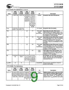
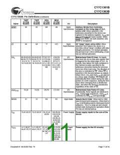
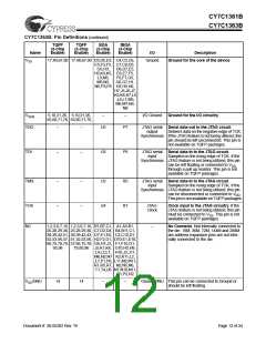
CY7C1361B
CY7C1363B
Single Write Accesses Initiated by ADSC
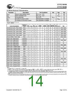
Functional Overview
All synchronous inputs pass through input registers controlled
by the rising edge of the clock. Maximum access delay from
the clock rise (tC0) is 6.5 ns (133-MHz device).
The CY7C1361B/CY7C1363B supports secondary cache in
systems utilizing either a linear or interleaved burst sequence.
The interleaved burst order supports Pentium® and i486
processors. The linear burst sequence is suited for processors
that utilize a linear burst sequence. The burst order is
user-selectable, and is determined by sampling the MODE
input. Accesses can be initiated with either the Processor
Address Strobe (ADSP) or the Controller Address Strobe
(ADSC). Address advancement through the burst sequence is
This write access is initiated when the following conditions are
satisfied at clock rise: (1) CE1, CE2, and CE3[2] are all asserted
active, (2) ADSC is asserted LOW, (3) ADSP is deasserted
HIGH, and (4) the write input signals (GW, BWE, and BWX)
indicate a write access. ADSC is ignored if ADSP is active LOW.
The addresses presented are loaded into the address register
and the burst counter/control logic and delivered to the
memory core. The information presented to DQ[A:D] will be
written into the specified address location. Byte writes are
allowed. All I/Os are three-stated when a write is detected,
even a byte write. Since this is a common I/O device, the
asynchronous OE input signal must be deasserted and the
I/Os must be three-stated prior to the presentation of data to
DQs. As a safety precaution, the data lines are three-stated
controlled by the ADV input. A two-bit on-chip wraparound
burst counter captures the first address in a burst sequence
and automatically increments the address for the rest of the
burst access.
once a write cycle is detected, regardless
of the state of OE.
Burst Sequences
Byte write operations are qualified with the Byte Write Enable
The CY7C1361B/CY7C1363B provides an on-chip two-bit
wraparound burst counter inside the SRAM. The burst counter
is fed by A[1:0], and can follow either a linear or interleaved
burst order. The burst order is determined by the state of the
MODE input. A LOW on MODE will select a linear burst
sequence. A HIGH on MODE will select an interleaved burst
order. Leaving MODE unconnected will cause the device to
default to a interleaved burst sequence.
X
(BWE) and Byte Write Select (BW ) inputs. A Global Write
Enable (GW) overrides all byte write inputs and writes data to
all four bytes. All writes are simplified with on-chip
synchronous self-timed write circuitry.
Three synchronous Chip Selects (CE1, CE2, CE3[2]) and an
asynchronous Output Enable (OE) provide for easy bank
selection and output three-state control. ADSP is ignored if
CE1 is HIGH.
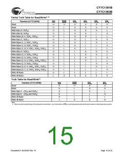
Interleaved Burst Address Table
(MODE = Floating or VDD)
Single Read Accesses
A single read access is initiated when the following conditions
First
Second
Address
A1: A0
Third
Address
A1: A0
Fourth
Address
A1: A0
[2]
are satisfied at clock rise: (1) CE1, CE2, and CE3 are all
Address
A1: A0
asserted active, and (2) ADSP or ADSC is asserted LOW (if
the access is initiated by ADSC, the write inputs must be
deasserted during this first cycle). The address presented to
the address inputs is latched into the address register and the
burst counter/control logic and presented to the memory core.
If the OE input is asserted LOW, the requested data will be
available at the data outputs a maximum to tCDV after clock
rise. ADSP is ignored if CE1 is HIGH.
00
01
10
11
01
00
11
10
10
11
00
01
11
10
01
00
Linear Burst Address Table (MODE = GND)
First
Second
Address
A1: A0
Third
Address
A1: A0
Fourth
Address
A1: A0
Single Write Accesses Initiated by ADSP
Address
A1: A0
This access is initiated when the following conditions are
[2]
satisfied at clock rise: (1) CE1, CE2, CE3 are all asserted
00
01
10
11
01
10
11
00
10
11
00
01
11
00
01
10
active, and (2) ADSP is asserted LOW. The addresses
presented are loaded into the address register and the burst
inputs (GW, BWE, and BWX)are ignored during this first clock
cycle. If the write inputs are asserted active (see Write Cycle
Descriptions table for appropriate states that indicate a write)
on the next clock rise, the appropriate data will be latched and
written into the device.Byte writes are allowed. All I/Os are
three-stated during a byte write.Since this is a common I/O
device, the asynchronous OE input signal must be deasserted
and the I/Os must be three-stated prior to the presentation of
data to DQs. As a safety precaution, the data lines are
three-stated once a write cycle is detected, regardless of the
state of OE.
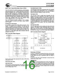
Sleep Mode
The ZZ input pin is an asynchronous input. Asserting ZZ
places the SRAM in a power conservation “sleep” mode. Two
clock cycles are required to enter into or exit from this “sleep”
mode. While in this mode, data integrity is guaranteed.
Accesses pending when entering the “sleep” mode are not
considered valid nor is the completion of the operation
guaranteed. The device must be deselected prior to entering
“sleep” mode. CE , CE , CE [2], ADSP, and ADSC must
the
1
2
3
remain inactive for the duration of tZZREC after the ZZ input
returns LOW.
Document #: 38-05302 Rev. *B
Page 13 of 34

 CYPRESS [ CYPRESS ]