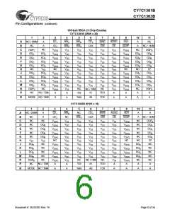
CY7C1361B
CY7C1363B
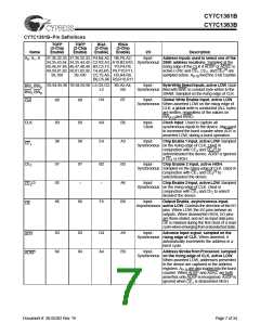
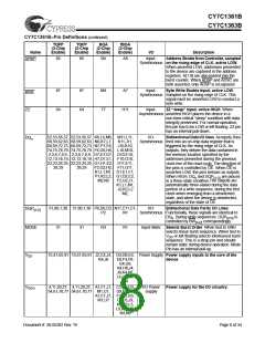
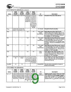
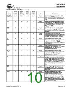
CY7C1363B: Pin Definitions (continued)
TQFP
(3-Chip
Enable)
TQFP
(2-Chip
Enable)
BGA
fBGA
(3-Chip
Enable)
(2-Chip
Enable)
Name
I/O
Description
93,94
88
93,94
88
L5,G3
H4
B5,A4
Input-
Byte Write Select Inputs, active LOW.
BWA,BWB
Synchronous Qualified with BWE to conduct byte writes
to the SRAM. Sampled on the rising edge of
CLK.
B7
Input-
Global Write Enable Input, active LOW.
GW
Synchronous When asserted LOW on the rising edge of
CLK, a global write is conducted (ALL bytes
are written, regardless of the values on
BW[A:B] and BWE).
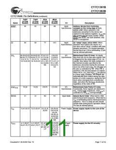
87
89
98
87
89
98
M4
K4
E4
A7
B6
A3
Input-
Byte Write Enable Input, active LOW.
BWE
CLK
Synchronous Sampled on the rising edge of CLK. This
signal must be asserted LOW to conduct a
byte write.
Input-
Clock
Clock Input. Used to capture all
synchronous inputs to the device. Also used
to increment the burst counter when ADV is
asserted LOW, during a burst operation.
Input-
Chip Enable 1 Input, active LOW.
CE1
CE2
Synchronous Sampled on the rising edge of CLK. Used in
conjunction with CE2 and CE3[2] to
select/deselect the device. ADSP is ignored
if CE1 is HIGH.
97
92
86
97
–
B2
–
B3
A6
B8
Input-
Chip Enable 2 Input, active HIGH.
Synchronous Sampled on the rising edge of CLK. Used in
conjunction with CE1 and CE3[2] to
select/deselect the device.
[2]
Input-
Chip Enable 3 Input, active LOW.
CE3
Synchronous Sampled on the rising edge of CLK. Used in
conjunction with CE1 and CE2 to
select/deselect the device.
86
F4
Input-
Output Enable, asynchronous input,
OE
Asynchronous active LOW. Controls the direction of the
I/O pins. When LOW, the I/O pins behave as
outputs. When deasserted HIGH, I/O pins
are three-stated, and act as input data pins.
OE is masked during the first clock of a read
cycle when emerging from a deselected
state.
83
84
83
84
G4
A4
A9
B9
Input-
Advance Input signal, sampled on the
ADV
Synchronous rising edge of CLK. When asserted, it
automatically increments the address in a
burst cycle.
Input-
Address Strobe from Processor,
ADSP
Synchronous sampled on the rising edge of CLK,
active LOW. When asserted LOW,
addresses presented to the device are
captured in the address registers. A[1:0] are
also loaded into the burst counter. When
ADSP and ADSC are both asserted, only
ADSP is recognized. ASDP is ignored when
CE1 is deasserted HIGH.
Document #: 38-05302 Rev. *B
Page 10 of 34

 CYPRESS [ CYPRESS ]