CY7C1361B
CY7C1363B
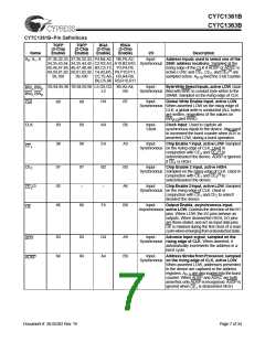
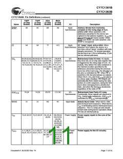
CY7C1361B–Pin Definitions
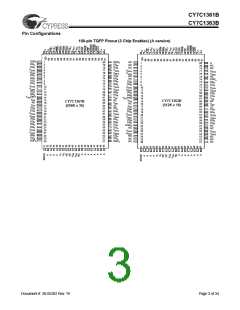
TQFP
(3-Chip
Enable)
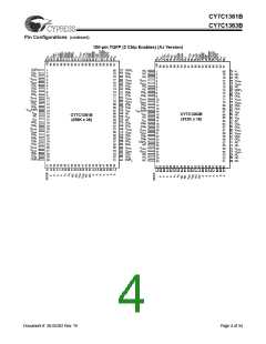
TQFP
(2-Chip
Enable)
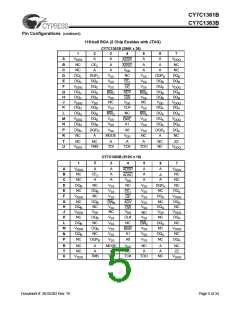
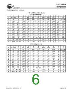
BGA
fBGA
(3-Chip
Enable)
(2-Chip
Enable)
Name
A0, A1, A
I/O
Input-
Description
Address Inputs used to select one of the
37,36,32,33, 37,36,32,33, P4,N4,A2, R6,P6,A2,
34,35,43,44, 34,35,44,45, C2,R2,A3, A10,B2,B10, Synchronous 256K address locations. Sampled at the
45,46,47,48, 46,47,48,49, B3,C3,T3, P3,P4,P8,
49,50,81,82, 50,81,82,92, T4,A5,B5, P9,P10,P11,
rising edge of the CLK if ADSP or ADSC is
active LOW, and CE1, CE2, and CE3[2] are
sampled active. A[1:0] feed the 2-bit counter.
99,100
99,100
C5,T5,A6, R3,R4,R8,
B6,C6,R6 R9,R10,R11
93,94,95,96 93,94,95,96 L5,G5,G3, B5,A5,A4,
Input-
Byte Write Select Inputs, active LOW. Qual-
BWA,BWB
BWC,BWD
L3
B4
Synchronous ified with BWE to conduct byte writes to the
SRAM. Sampled on the rising edge of CLK.
H4
B7
Input-
Global Write Enable Input, active LOW.
88
88
GW
Synchronous When asserted LOW on the rising edge of
CLK, a global write is conducted (ALL bytes
are written, regardless of the values on
BW[A:D]and BWE).
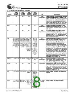
CLK
CE1
CE2
89
98
89
98
K4
E4
B6
A3
Input-
Clock Input. Used to capture all
Clock
synchronous inputs to the device. Also used
to increment the burst counter when ADV is
asserted LOW, during a burst operation.
Input-
Chip Enable 1 Input, active LOW. Sampled
Synchronous on the rising edge of CLK. Used in
conjunction with CE2 and CE3[2] to
select/deselect the device. ADSP is ignored
if CE1 is HIGH.
97
92
86
97
–
B2
–
B3
A6
B8
Input-
Chip Enable 2 Input, active HIGH.
Synchronous Sampled on the rising edge of CLK. Used in
conjunction with CE1 and CE3[2] to
select/deselect the device.
[2]
Input-
Chip Enable 3 Input, active LOW. Sampled
CE3
Synchronous on the rising edge of CLK. Used in
conjunction with CE1 and CE2 to select/
deselect the device.
86
F4
Input-
Output Enable, asynchronous input,
OE
Asynchronous active LOW. Controls the direction of the I/O
pins. When LOW, the I/O pins behave as
outputs. When deasserted HIGH, I/O pins
are three-stated, and act as input data pins.
OE is masked during the first clock of a read
cyclewhenemergingfromadeselectedstate.
83
84
83
84
G4
A4
A9
B9
Input-
Advance Input signal, sampled on the
ADV
Synchronous rising edge of CLK. When asserted, it
automatically increments the address in a
burst cycle.
Input-
Address Strobe from Processor, sampled
ADSP
Synchronous on the rising edge of CLK, active LOW.
When asserted LOW, addresses presented
to the device are captured in the address
registers. A[1:0] are also loaded into the burst
counter. When ADSP and ADSC are both
asserted, only ADSP is recognized. ASDP is
ignored when
is deasserted HIGH.
CE1
Document #: 38-05302 Rev. *B
Page 7 of 34

 CYPRESS [ CYPRESS ]