CY7C1361B
CY7C1363B
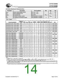
ZZ Mode Electrical Characteristics
Parameter
IDDZZ
tZZS
Description
Snooze mode standby current
Device operation to ZZ
Test Conditions
ZZ > VDD – 0.2V
ZZ > VDD – 0.2V
Min.
Max.
35
2tCYC
Unit
mA
ns
tZZREC
tZZI
tRZZI
ZZ recovery time
ZZ active to snooze current
ZZ Inactive to exit snooze current
ZZ < 0.2V
This parameter is sampled
This parameter is sampled
2tCYC
0
ns
ns
ns
2tCYC
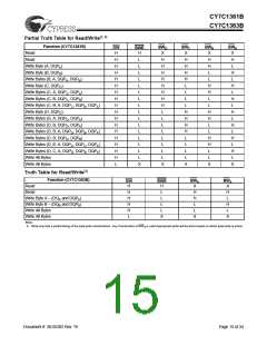
Truth Table[ 3, 4, 5, 6, 7]
Address
Cycle Description
Used CE1 CE2 CE3 ZZ ADSP
ADSC ADV WRITE OE CLK
DQ
Deselected Cycle, Power-down None
Deselected Cycle, Power-down None
Deselected Cycle, Power-down None
Deselected Cycle, Power-down None
Deselected Cycle, Power-down None
H
L
L
L
X
X
L
L
L
L
L
X
L
X
L
X
X
X
X
H
X
X
X
L
L
L
L
L
X
X
X
X
X
X
X
X
X
X
X
X
L
L
L
L
L
H
L
L
L
L
L
L
L
L
L
L
L
L
L
L
L
L
L
X
L
L
H
H
X
L
L
H
H
H
H
H
X
X
H
X
H
H
X
X
H
X
L
X
X
L
L
X
X
X
L
L
L
X
X
X
X
X
X
X
X
X
X
X
L
L
L
L
L
L
X
X
X
X
X
X
X
X
L
H
H
H
H
H
H
L
X
X
X
X
X
X
L
H
X
L
H
L
H
L
H
X
X
L
H
L
L-H three-state
L-H three-state
L-H three-state
L-H three-state
L-H three-state
Snooze Mode, Power-down
None
X
L-H
three-state
Q
Read Cycle, Begin Burst
Read Cycle, Begin Burst
Write Cycle, Begin Burst
Read Cycle, Begin Burst
Read Cycle, Begin Burst
Read Cycle, Continue Burst
Read Cycle, Continue Burst
Read Cycle, Continue Burst
External
External
External
External
External
Next
H
H
H
H
H
X
X
X
X
X
X
X
X
X
X
X
X
L-H three-state
L-H
L-H
D
Q
L-H three-state
L-H
L-H three-state
L-H
L-H three-state
X
X
H
H
H
H
Q
Next
Next
Q
Read Cycle, Continue Burst
Write Cycle, Continue Burst
Write Cycle, Continue Burst
Read Cycle, Suspend Burst
Read Cycle, Suspend Burst
Read Cycle, Suspend Burst
Read Cycle, Suspend Burst
Write Cycle, Suspend Burst
Next
Next
Next
Current
Current
Current
Current
Current
Current
H
X
H
X
X
H
H
X
H
H
H
H
H
H
H
H
H
H
L-H
L-H
L-H
D
D
Q
L
H
H
H
H
H
H
H
H
H
H
L
L-H three-state
L-H
L-H three-state
Q
H
X
X
L-H
L-H
D
D
Write Cycle, Suspend Burst
L
Notes:
3. X=”Don't Care.” H = Logic HIGH, L = Logic LOW.
4. WRITE = L when any one or more Byte Write enable signals and BWE = L or GW= L. WRITE = H when all Byte write enable signals, BWE, GW = H.
5. The DQ pins are controlled by the current cycle and the signal. is asynchronous and is not sampled with the clock.
OE
OE
must be driven HIGH prior to the start of the write cycle to allow the outputs to three-state.
6. The SRAM always initiates a read cycle when ADSP is asserted, regardless of the state of GW, BWE, or BW . Writes may occur only on subsequent clocks after
X
the
or with the assertion of
. As a result,
is a don't
OE
ADSC
OE
ADSP
care for the remainder of the write cycle.
7.
is asynchronous and is not sampled with the clock rise. It is masked internally during write cycles. During a read cycle all data bits are three-state when
OE
is
OE
inactive or when the device is deselected, and all data bits behave as output when
is active (LOW).
OE
3
Document #: 38-05302 Rev. *B
Page 14 of 34

 CYPRESS [ CYPRESS ]