AIS Baseband Processor
CMX910
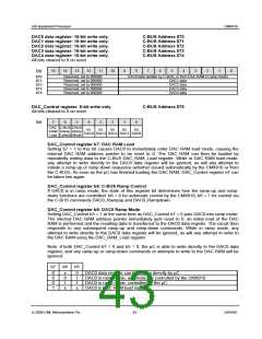
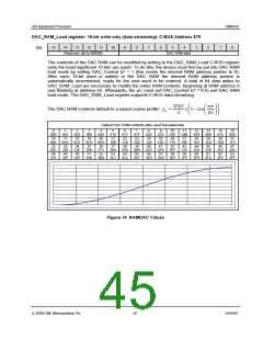
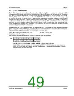
DAC_RAM_Load register: 16-bit write only (data-streaming). C-BUS Address $79
15
14
13
12
11
10
9
8
7
6
5
4
3
2
1
0
Bit:
Reserved, set to 000000
DAC RAM data
The contents of the DAC RAM can be modified by writing to the DAC_RAM_Load C-BUS register
(only the least significant 10 bits are used). To do this, the device must first be put into DAC RAM
load mode by setting DAC_Control b7 = 1 (this resets the internal RAM address pointer to 0).
After each 10-bit word is written to the DAC RAM the internal RAM address pointer is
automatically incremented, ready for the next word to be entered. A total of 64 data writes to
DAC_RAM_Load are necessary to modify the entire RAM contents, beginning at RAM address 0
and finishing at address 63. Afterwards, the µC must set DAC_Control b7 = 0 to exit DAC RAM
load mode. The DAC_RAM_Load register supports C-BUS data-streaming.
1023 ⎛
×⎜1− cos
nπ ⎞
⎛
⎝
⎞
The DAC RAM contents default to a raised cosine profile: yn =
⎟
⎟
⎜
⎟
⎠
⎜
2
63
⎝
⎠
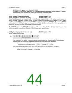
Default DAC RAM contents after reset (hexadecimal)
0
000
16
1
001
17
2
003
18
3
006
19
4
00A
20
5
010
21
6
017
22
7
01F
23
8
028
24
9
033
25
10
03E
26
11
04B
27
12
059
28
13
068
29
14
078
30
15
089
31
09A
32
20C
0AD 0C1
0D5
35
258
0EA
36
271
100
37
28A
116
38
2A2
12D
39
2BA
145
40
2D2
15D
41
2E9
175
42
2FF
58
18E
43
315
59
1A7
44
32A
60
1C0
45
33E
1D9
46
352
1F3
47
365
63
33
226
49
34
23F
50
48
51
52
53
54
55
56
57
61
62
376
387
397
3A6
3B4
3C1 3CC 3D7
3E0
3E8
3EF
3F5
3F9
3FC
3FE
3FF
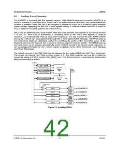
Figure 14 RAMDAC Values
© 2009 CML Microsystems Plc
45
D/910/6

 CMLMICRO [ CML MICROCIRCUITS ]