AIS Baseband Processor
CMX910
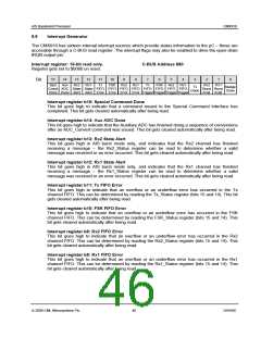
5.8
Auxiliary D-to-A Converters
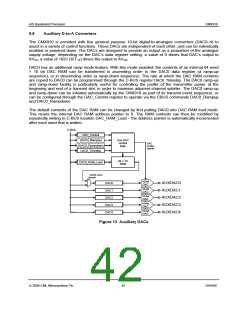
The CMX910 is provided with five general purpose 10-bit digital-to-analogue converters (DAC0–4) to
assist in a variety of control functions. These DACs are independent of each other, and can be individually
enabled or powered down. The DACs are designed to provide an output as a proportion of the analogue
supply voltage, depending on the DAC’s data register setting: a value of 0 drives that DAC’s output to
AVSS; a value of 1023 (3FF16) drives the output to AVDD.
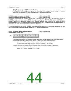
DAC0 has an additional ramp mode feature. With this mode enabled, the contents of an internal 64 word
× 10 bit DAC RAM can be transferred in ascending order to the DAC0 data register (a ramp-up
sequence), or in descending order (a ramp-down sequence). The rate at which the DAC RAM contents
are copied to DAC0 can be programmed through the C-BUS register DAC0_Timestep. The DAC0 ramp-up
and ramp-down facility is particularly useful for controlling the profile of the transmitter power at the
beginning and end of a transmit slot, in order to minimise adjacent-channel splatter. The DAC0 ramp-up
and ramp-down can be initiated automatically by the CMX910 as part of its transmit event sequencer, or
can be configured through the DAC_Control register to operate via the CBUS commands DAC0_Rampup
and DAC0_Rampdown.
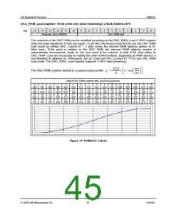
The default contents of the DAC RAM can be changed by first putting DAC0 into DAC RAM load mode.
This resets the internal DAC RAM address pointer to 0. The RAM contents can then be modified by
repeatedly writing to C-BUS location DAC_RAM_Load – the address pointer is automatically incremented
after each word that is written.
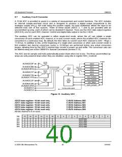
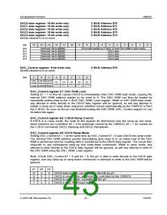
C-BUS
DAC_Control
(DAC0_Rampup)
(DAC0_Rampdown)
DAC0_Timestep
Aux DAC
control
logic
DAC
enable
signals
64 x 10
RAM
DAC0_RAM_Load
DAC0 ramp
mode
DAC0
DAC1
DAC2
DAC3
DAC4
AUXDAC0
AUXDAC1
AUXDAC2
AUXDAC3
AUXDAC4
Figure 13 Auxiliary DACs
© 2009 CML Microsystems Plc
42
D/910/6

 CMLMICRO [ CML MICROCIRCUITS ]