AIS Baseband Processor
CMX910
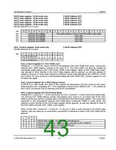
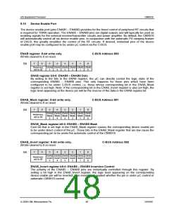
DAC_Control register b4-0: Enable DAC4-0
Writing a 1 to these bits powers up the corresponding DAC analogue circuit, writing a 0 powers
down the DAC and puts the DAC output pin into a high impedance state.
DAC0_Rampup command (no data)
DAC0_Rampdown command (no data)
C-BUS Address $76
C-BUS Address $77
These two commands are enabled only if DAC_Control register b7-5 = 011. In that case, issuing a
DAC0_Rampup command causes DAC0 to begin ramping up (RAM[0→63] copied to DAC0 data
register), and DAC0_Rampdown causes DAC0 to begin ramping down (RAM [63→0] copied to DAC0
data register). If a DAC0_Rampup command is issued while DAC0 is in the process of ramping down, or
vice-versa, the ramp process immediately reverses direction.
The CMX910 ignores any DAC0_Rampup commands issued when DAC0 is already ramped up, or any
DAC0_Rampdown commands issued when DAC0 is already ramped down.
DAC0_Timestep register: 8-bit write only.
C-BUS Address $78
All bits cleared to 0 on reset.
7
6
5
4
3
2
1
0
Bit:
DAC0 ramp timestep
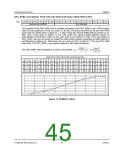
The contents of the DAC0_Timestep register determine the rate at which the DAC RAM data is
transferred to the DAC0 data register during a ramp-up or ramp-down sequence:
Time between each data transfer = (DAC0_Timestep + 1) × 0.25µs
The time taken for the entire ramp-up or ramp-down process to complete is therefore:
tRAMP = 63 × (DAC0_Timestep + 1) × 0.25µs
© 2009 CML Microsystems Plc
44
D/910/6

 CMLMICRO [ CML MICROCIRCUITS ]