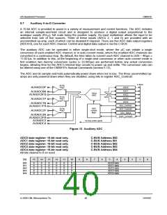
AIS Baseband Processor
CMX910
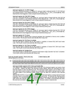
DAC0 data register: 16-bit write only.
DAC1 data register: 16-bit write only.
DAC2 data register: 16-bit write only.
DAC3 data register: 16-bit write only.
DAC4 data register: 16-bit write only.
All bits cleared to 0 on reset.
C-BUS Address $70
C-BUS Address $71
C-BUS Address $72
C-BUS Address $73
C-BUS Address $74
15
14
13
12
11
10
9
8
7
6
5
4
3
2
1
0
Bit:
$70:
$71:
$72:
$73:
$74:
Reserved, set to 000000
Reserved, set to 000000
Reserved, set to 000000
Reserved, set to 000000
Reserved, set to 000000
DAC0 data (written by C-BUS, or from DAC RAM in ramp mode)
DAC1 data
DAC2 data
DAC3 data
DAC4 data
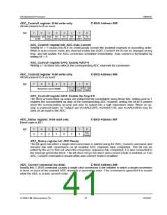
DAC_Control register: 8-bit write only.
C-BUS Address $75
All bits cleared to 0 on reset.
7
6
5
4
3
2
1
0
Bit:
DAC C-BUS DAC0
RAM Ramp Ramp
Load Control Mode
En
En
En
En
En
DAC4 DAC3 DAC2 DAC1 DAC0
DAC_Control register b7: DAC RAM Load
Setting b7 = 1 to this bit causes DAC0 to immediately enter DAC RAM load mode, causing the
internal DAC RAM address pointer to be reset to 0. The DAC RAM can then be loaded by
repeatedly writing data to the C-BUS DAC_RAM_Load register. While in DAC RAM load mode,
any attempt to write directly to the DAC0 data register will be ignored, as will any attempt to
initiate a ramp-up or ramp-down sequence (whether issued automatically by the CMX910 or from
the C-BUS). As soon as the µC has finished loading the DAC RAM, DAC_Control register b7 can
be taken low again.
DAC_Control register b6: C-BUS Ramp Control
If DAC0 is in ramp mode, the state of this register bit determines how the ramp-up and ramp-
down functions are controlled: b6 = 0 for automatic control by the CMX910, b6 = 1 for control via
the C-BUS commands DAC0_Rampup and DAC0_Rampdown.
DAC_Control register b5: DAC0 Ramp Mode
Setting DAC_Control b5 = 1 at the same time as DAC_Control b7 = 0 puts DAC0 into ramp mode.
The internal DAC RAM address pointer immediately gets reset to 0, an initial read of the DAC
RAM is performed and the resulting data is transferred to the DAC0 data register. The circuit then
responds to any subsequent ramp-up and ramp-down commands. While in ramp mode, any
attempt to write directly to the DAC0 data register will be ignored, as will any attempt to write to
the DAC RAM using the DAC_RAM_Load register.
Note: if both DAC_Control b7 = 0 and b5 = 0, the µC is able to write directly to the DAC0 data
register, and any ramp-up or ramp-down commands or attempts to write to the DAC RAM will be
ignored:
b7
b6
b5
0
0
0
1
x
0
1
x
0
1
1
x
DAC0 data register can be written directly by µC
DAC0 in ramp mode, automatically controlled by the CMX910
DAC0 in ramp mode, controlled by the µC
DAC0 in DAC RAM load mode
© 2009 CML Microsystems Plc
43
D/910/6

 CMLMICRO [ CML MICROCIRCUITS ]