AIS Baseband Processor
CMX910
5.7
Auxiliary A-to-D Converter
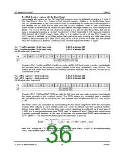
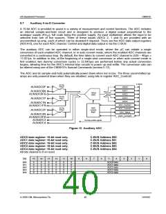
A 10-bit ADC is provided to assist in a variety of measurement and control functions. The ADC includes
an internal sample-and-hold circuit and is designed to produce a digital output proportional to the
analogue supply (AVDD), full scale being the positive supply. An input multiplexer allows the input to be
selected from one of five sources. Three of these inputs (ADCs 2, 1 and 0) are provided with an
uncommitted op-amp, each of which can be disabled if required. There are five ADC data output registers
(ADC4-0), one for each ADC channel. Control and digital data output is via the C-BUS.
The auxiliary ADC can be operated in either single-shot mode, where the µC can initiate a single
conversion of each enabled ADC channel, or in auto convert mode, where the enabled ADC channels are
converted in a continuous loop. By default, the time taken to convert each ADC channel is (529 ÷ 48)µs ≈
11.021µs. In addition to this, at the beginning of a single-shot conversion or when auto convert mode is
first enabled, two dummy conversion cycles (≈ 22.042µs) are performed before any actual conversion
begins, allowing time for the ADC’s internal bias circuits to power up and settle. The conversion rate can
be altered using one of the CMX910’s Special Commands (section 5.12).
The ADC and its sample-and-hold automatically power down when not in use. The three uncommitted op-
amps are only powered down when they are disabled, using bits in register ADC_Control2.
C-BUS
En Op
Amp 0
AUXADC0P
ADC0
ADC1
AUXADC0N
AUXADC0FB
ADC2
En Op
Amp 1
ADC3
AUXADC1P
ADC4
AUXADC1N
ADC_Control1
ADC_Control2
ADC_Status
(ADC_Convert)
AUXADC1FB
En Op
Amp 2
AUXADC2P
AUXADC2N
AUXADC2FB
AUXADC3
Op Amp enable signals
AUXADC4
Figure 12 Auxiliary ADC
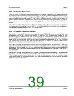
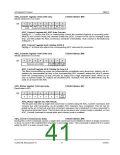
ADC0 data register: 16-bit read only.
ADC1 data register: 16-bit read only.
ADC2 data register: 16-bit read only.
ADC3 data register: 16-bit read only.
ADC4 data register: 16-bit read only.
All bits cleared to 0 on reset.
C-BUS Address $60
C-BUS Address $61
C-BUS Address $62
C-BUS Address $63
C-BUS Address $64
15
14
13
12
11
10
9
8
7
6
5
4
3
2
1
0
Bit:
$60:
$61:
$62:
$63:
$64:
0
0
0
0
0
0
0
0
0
0
0
0
0
0
0
0
0
0
0
0
0
0
0
0
0
0
0
0
0
0
ADC0 data
ADC1 data
ADC2 data
ADC3 data
ADC4 data
© 2009 CML Microsystems Plc
40
D/910/6

 CMLMICRO [ CML MICROCIRCUITS ]