AIS Baseband Processor
CMX910
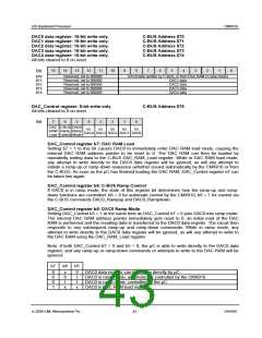
5.6.4 DSC Receive (Main Channel)
Either the Rx1 or Rx2 channel can be configured for DSC reception. The CMX910 first applies 6dB/octave
de-emphasis to the received signal, then demodulates the resulting 1200 baud NRZ FSK data. Only one
of the channels at a time must be configured for DSC reception. The received data is packed into 8-bit
bytes for forward transmission to the µC. The CMX910 makes no attempt to align data bits within the
bytes or perform dot pattern or data phasing detection, those functions must be performed by the host µC.
No attempt is made to correctly align data, it is simply packed into bytes (least significant bit first) as it
arrives.
Note: when the Rx1 or Rx2 channel is configured for DSC operation, the received data is forwarded to the
µC through FSK_FIFO, not Rx1_FIFO or Rx2_FIFO. This prevents the DSC reception from corrupting any
AIS data that may still be present in Rx1_FIFO or Rx2_FIFO.
5.6.5 DSC Receive (External FSK Interface)
The CMX910’s external FSK interface retimes asynchronous NRZ FSK data from an external 1200 baud
demodulator such as the FX604, and is intended for use as a third parallel receive channel for DSC
reception in the case that both of the main receive channels are assigned to AIS operation. The data from
the external FSK demodulator is applied to the FSK_RXD pin and gets packed into 8-bit bytes (least
significant bit first) before being loaded into FSK_FIFO for forward transmission to the µC. The CMX910’s
FSK interface circuit does not align data bits within the bytes or perform dot pattern or data phasing
detection, those functions must be performed by the host µC.
Two further input pins are provided to prevent data from being decoded in the absence of a valid FSK
signal: the FSK_MUTE input is intended for connection to the DSC radio sub-system, and should go high
to indicate no received signal; the FSK_DET input is intended for connection to the FSK demodulator and
indicates that valid FSK data is being received. Data will only be written to the FSK FIFO if FSK_MUTE =
0 and FSK_DET = 1.
The CMX910 samples data on the FSK_RXD pin half a bit period after each transition (i.e. in the middle of
a received bit), and every bit period thereafter until another transition occurs. A transition on the
FSK_RXD pin should occur at least once in every ten bit periods in order to maintain reliable
synchronisation with the incoming bit stream. The CMX910’s data retiming circuit can tolerate an error of
1.5% in the input data baud rate.
© 2009 CML Microsystems Plc
39
D/910/6

 CMLMICRO [ CML MICROCIRCUITS ]