AIS Baseband Processor
CMX910
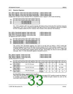
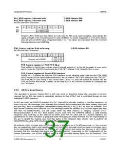
Rx1/Rx2_Control register b0: Rx State Reset
Immediately after power up, the Rx1 and Rx2 channels must be initialised by writing a 1 to bit 0
(Rx State Reset) of the Rx1_Control or Rx2_Control registers. Writing a 1 to the Rx State Reset
bits can also be done at any other time in order to immediately terminate an active reception in
that channel and to cause the Rx state (AIS raw or burst mode) to revert to “Idle”. Any internal
states related to receive will be cleared and the internal message buffers (AIS burst mode) will be
wiped. The receive FIFOs are not cleared by writing a 1 to the Rx State Reset bits, that can be
done if necessary by writing a 1 to Rx1_Control bit 1 or Rx2_Control bit 1 (AIS raw/burst mode) or
FSK_Control bit 1 (DSC mode). Note: after a 1 is written to bit 0 of the Rx1_Control (or
Rx2_Control), it will take up to 250µs before that channel is reset properly and data stops being
written to the associated FIFO (Rx1_FIFO, Rx2_FIFO, or FSK_FIFO). Only after that time should
the FIFO be cleared or the Rx1_Control (or Rx2_Control) register be written to again.
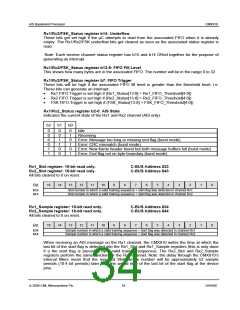
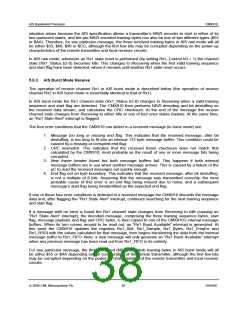
Rx1_FreqErr register: 16-bit read only.
Rx2_FreqErr register: 16-bit read only.
All bits cleared to 0 on reset.
C-BUS Address $37
C-BUS Address $47
15
14
13
12
11
10
9
8
7
6
5
4
3
2
1
0
Bit:
$37:
$47:
Rx1 channel frequency error (Hz)
Rx2 channel frequency error (Hz)
Registers Rx1_FreqErr and Rx2_FreqErr are only valid for AIS burst mode reception, and indicate
the frequency error of the received carrier (relative to the local oscillator) in units of Hertz. The
values are calculated from the received training sequence and start flag and are reported in 2’s
complement format.
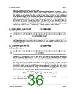
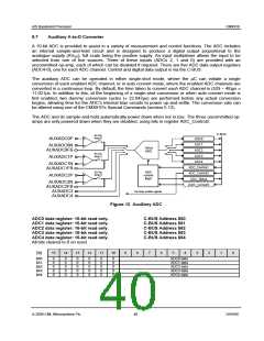
Rx1_RSSI register: 16-bit read only.
Rx2_RSSI register: 16-bit read only.
All bits cleared to 0 on reset.
C-BUS Address $38
C-BUS Address $48
15
14
13
12
11
10
9
8
7
6
5
4
3
2
1
0
Bit:
$38:
$48:
Rx1 channel RSSI
Rx2 channel RSSI
Registers Rx1_RSSI and Rx2_RSSI are valid for AIS burst and raw mode reception, and indicate
the signal strength of the received carrier. The RSSI values are calculated over a specified
window within each slot, as set up by the “rssi_window” special command function (see section
5.12).
The RSSI values are calculated by accumulating the I/Q vector magnitudes from the associated
channel filter outputs at each sample point (i.e. every 20.833µs) over the specified window.
Before being added to the running total, each vector magnitude is multiplied by a fixed gain of
0.4117 and a user-programmable gain “RSSI_gain” of between 0 and 1 (this is also set up using
a special command function). In the case of overflow, the accumulated RSSI value saturates at
32767 ($7FFF). The total accumulated signal strength value is given by:
RSSI _ start+length−2
2
2
⎛
⎜
⎞
⎟
RSSI =
I + Q ×0.4117× RSSI _ gain
∑
n
n
⎝
⎠
n=RSSI _ start
With a DC voltage of ±1.7V (differential) applied to the input of the I or Q ADC, the corresponding
I or Q channel filter output will be approximately ±30000.
© 2009 CML Microsystems Plc
36
D/910/6

 CMLMICRO [ CML MICROCIRCUITS ]