AIS Baseband Processor
CMX910
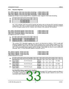
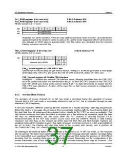
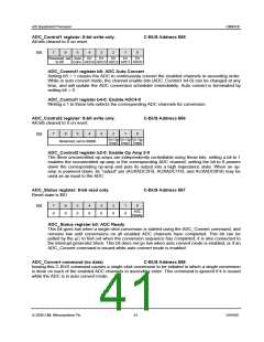
Rx1_RSSI register: 8-bit read only.
Rx2_RSSI register: 8-bit read only.
All bits cleared to 0 on reset.
C-BUS Address $38
C-BUS Address $48
7
6
5
4
3
2
1
0
Bit:
$38:
$48:
Rx1 channel RSSI
Rx2 channel RSSI
Registers Rx1_RSSI and Rx2_RSSI are only valid for AIS burst mode reception, and indicate the
signal strength of the received carrier in units of dB (an I/Q vector magnitude of 0.5V at the device
pins will give an RSSI value of approximately 112). The values are calculated from the received
training sequence and start flag.
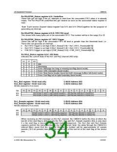
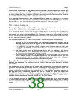
FSK_Control register: 8-bit write only.
C-BUS Address $53
All bits cleared to 0 on reset.
7
6
5
4
3
2
1
0
Bit:
FSK
En
Reserved, set to 000000
FIFO FSK
Clear I/F
FSK_Control register b1: FSK FIFO Clear
Data written to this bit does not get stored; instead, writing a 1 to this bit generates a reset pulse
which clears the FSK FIFO and resets the FSK FIFO fill level (FSK_Status b13-8) to zero.
FSK_Control register b0: Enable FSK Interface
Setting b0 = 1 enables the external FSK interface circuit, allowing serial data from the FSK_RXD
pin to be packed into bytes and transferred to the µC via the FSK_FIFO (subject to the FSK_DET
and FSK_MUTE pins being in the correct state). If b0 = 0, data will instead be loaded into the
FSK_FIFO from whichever, if either, of the main Rx1 or Rx2 receive channels is configured for
DSC reception.
5.6.2 AIS Raw Mode Receive
The operation of receive channel Rx1 in AIS raw mode is described below (the operation of receive
channel Rx2 in AIS raw mode is essentially identical to that of Rx1, but is controlled through its own
individual C-BUS registers).
In AIS raw mode the CMX910 searches the Rx1 channel for a header (training + start flag sequence) to
detect the start of a message, then transfers the received data (starting with the three training bytes and
the start flag, then all subsequent demodulated bytes) directly to Rx1_FIFO as soon as available. This
byte stream continues even after the end of a message and in the absence of a received signal (the data
will then be indeterminate), but will cease while the Rx1 channel is sleeping (section 5.4.3).
Resynchronisation of the Rx1 data stream occurs each time the CMX910 detects a valid training
sequence and start flag on the channel (at which point the Rx1_Slot and Rx1_Sample registers are
updated) but no other indication is given that valid messages are being received; it is the responsibility of
the µC to detect the training and start flag bytes in the received data stream, and to perform all
HDLC/NRZI decoding, CRC checking and end flag detection.
Bit ordering of the received bytes in AIS raw mode is the same as in Tx AIS raw mode, i.e. the received
bits are packed into bytes most significant bit first. As the AIS message structure requires message bytes
to be transmitted least significant bit first, the µC must ensure that during the process of HDLC/NRZI
decoding that the resulting data bytes are correctly reversed. Depending on the configuration of the
remote transmitter, one of four different types of NRZI encoded training bytes may be received – this
© 2009 CML Microsystems Plc
37
D/910/6

 CMLMICRO [ CML MICROCIRCUITS ]