AIS Baseband Processor
CMX910
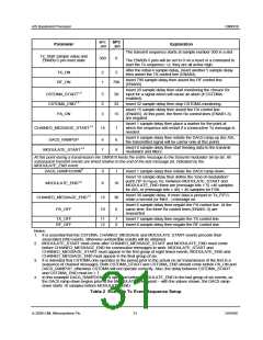
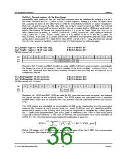
Rx1_Bytes register: 16-bit read only.
Rx2_Bytes register: 16-bit read only.
All bits cleared to 0 on reset.
C-BUS Address $35
C-BUS Address $45
15
14
13
12
11
10
9
8
7
6
5
4
3
2
1
0
Bit:
$35:
$45:
Number of message bytes received in channel Rx1 (AIS burst mode only)
Number of message bytes received in channel Rx2 (AIS burst mode only)
Registers Rx1_Bytes and Rx2_Bytes are only used in AIS burst mode and indicate the number of
message bytes that are available for the µC to read out.
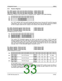
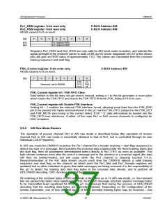
Rx1_Control register: 8-bit write only.
Rx2_Control register: 8-bit write only.
All bits cleared to 0 on reset.
C-BUS Address $36
C-BUS Address $46
7
6
5
4
3
2
1
0
Bit:
Rx1/2
Burst
Enab
Rx1
FIFO State
Clear Reset
Rx2
FIFO State
Clear Reset
Rx1
Rsvd, Rx1 DC offset
set to 0 correction
$36:
Rx1 mode
Rx2 mode
Rx2
Rsvd, Rx2 DC offset Rsvd,
set to 0 correction set to 0
$46:
Rx1/Rx2_Control register b6-5: DC offset correction
These bits are used to independently configure the I/Q DC offset correction mode for the Rx1 and
Rx2 channels.
b6
b5
0
0
1
1
0
1
0
1
I/Q DC offset correction: Reset and hold
I/Q DC offset correction: Hold
I/Q DC offset correction: Run slowly
I/Q DC offset correction: Run quickly
Rx1_Control register b4: Rx1 and Rx2 Burst Mode Enable
Bit 4 of the Rx1_Control register is used to select between burst and raw mode operation for both
the Rx1 and Rx2 channel (AIS only): b4 = 1 for burst mode, b4 = 0 for raw mode.
Rx1/Rx2_Control register b3-2: Rx1 and Rx2 Mode
These bits are used to independently configure the modulation type for the Rx1 and Rx2
channels.
b3
b2
0
0
1
1
0
1
0
1
AIS, 25kHz channel
AIS, 12.5kHz channel
DSC
Reserved, do not use
Rx1/Rx2_Control register b1: FIFO Clear
Data written to these bits do not get stored; instead, writing a 1 to either of these bits generates a
reset pulse which clears the Rx1 or Rx2 FIFO and resets the FIFO fill level (Rx1_Status or
Rx2_Status b13-8) to zero.
© 2009 CML Microsystems Plc
35
D/910/6

 CMLMICRO [ CML MICROCIRCUITS ]