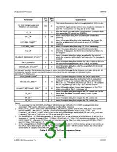
AIS Baseband Processor
CMX910
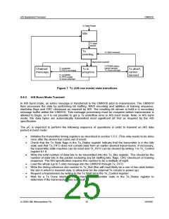
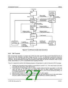
Tx State Reset
Idle
Tx abort,
message
too long
Buffer overflow
Tx Done interrupt
Write to Tx FIFO
Buffer overflow
Tx Done interrupt
Tx Start has been issued,
Start point reached
Tx Done interrupt
Building
message
buffer
Tx abort,
buffer not
ready
Message complete,
Tx Start not yet issued
Message complete,
Tx Start not yet reissued
Message
buffer
ready
Tx Start
issued
Message complete,
Tx Start has been issued
Message complete,
Tx Start has been reissued
Tx
pending
Tx Start reissued
Start point reached
CSTDMA active,
carrier sensed
Tx Done interrupt
Tx complete,
Tx FIFO not empty
Chained
message
Tx in
progress
Tx abort,
carrier
sensed
Tx complete,
Tx FIFO empty
Tx Done interrupt
Figure 8 Tx (AIS burst mode) state transitions
5.5.4 DSC Transmit
DSC transmission operates in a similar way to AIS raw mode: transmit data is passed directly from the Tx
FIFO to the FSK modulator and filters. Apart from the Tx FIFO, no buffering is performed inside the
CMX910. The µC must calculate the entire DSC transmit message including the dot pattern and phasing
sequence, and all subsequent message and checksum words (both DX and RX characters). Note: In DSC
mode, data written to Tx_FIFO is transmitted least significant bit first.
The µC is expected to perform the following sequence of operations in order to transmit a DSC message:
•
•
Initialise the transmitter timing registers as described in section 5.5.5. (This only needs to be done
once after the device has come out of reset).
Check that the Tx State flags in the Tx_Status register indicate that the transmitter is in the Idle
state and that the Tx FIFO does not contain data from an earlier aborted transmission. If
necessary, the transmitter state machine can be reset and Tx_FIFO can be cleared by writing 1 to
Tx_Control register b1-0.
•
•
Write the total number of bits to be transmitted into the Tx_Bits register.
Write the timing reference slot number to Tx_Slot (this will most likely be one or two slots before
the slot in which to transmit data, to allow time for the external Tx circuits to power up).
© 2009 CML Microsystems Plc
27
D/910/6

 CMLMICRO [ CML MICROCIRCUITS ]