AIS Baseband Processor
CMX910
•
Prime the Tx FIFO with at least one byte of transmit data, up to the entire message if it fits.
Unused bits in the last byte should be padded with zeroes – note that data written to the Tx_FIFO
in DSC mode is transmitted least significant bit first.
•
•
Request a transmission by writing to the Tx Start bit in the Tx_Control register.
Feed any remaining data bytes to the Tx FIFO as they are required, then wait for a Tx Done
interrupt and check the transmitter state in the Tx_Status register to determine if the transmission
was successful.
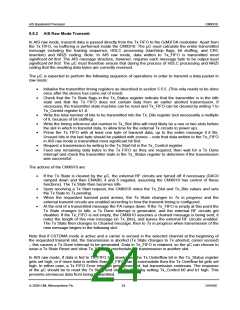
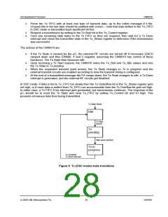
The actions of the CMX910 are:
•
If the Tx State is cleared by the µC, the external RF circuits are turned off if necessary (DAC0
ramped down and then ENAB0, 4 and 5 negated, assuming the CMX910 has control of these
functions). The Tx State then becomes Idle.
•
•
•
Upon receiving a Tx Start request, the CMX910 notes the Tx_Slot and Tx_Bits values and sets
the Tx State to Tx pending.
When the requested transmit point arrives, the Tx State changes to Tx in progress and the
external transmit circuits are enabled according to how the transmit timing is configured.
At the end of a transmitted message the PA ramps down, the Tx State changes to Idle, a Tx Done
interrupt is generated, and the external RF circuits get disabled.
In DSC mode, if data is fed to Tx_FIFO too slowly then the Tx Underflow bit in the Tx_Status register gets
set high, or if more data is written than Tx_FIFO can accommodate then the Tx Overflow bit gets set high.
In either case, a Tx FIFO Error interrupt gets generated, but transmission continues. The response of the
µC should be to reset the Tx State and clear Tx_FIFO by setting Tx_Control b0 and b1 high. This
prevents erroneous data from being transmitted.
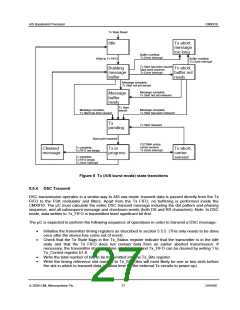
Tx State Reset
Idle
Tx Start
issued
Tx
pending
Start point reached
Tx in
progress
Tx complete
Tx Done interrupt
Figure 9 Tx (DSC mode) state transitions
© 2009 CML Microsystems Plc
28
D/910/6

 CMLMICRO [ CML MICROCIRCUITS ]