AIS Baseband Processor
CMX910
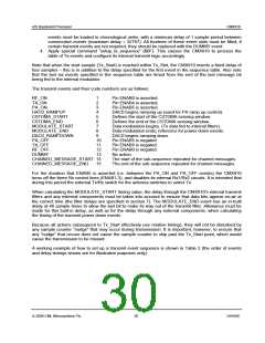
events must be loaded in chronological order, with a minimum delay of 1 sample period between
consecutive events (maximum delay = 32767). All fourteen of these event slots must be filled; if
certain transmit events are not required, they should be replaced with the DUMMY event.
4. Apply special command “setup_tx_sequence” ($0F). This causes the CMX910 to process the
table of Tx events and configure its internal transmit logic accordingly.
Note that when the start sample (Tx_Start) is reached within Tx_Slot, the CMX910 inserts a fixed delay of
four samples – this is in addition to the delay specified for the first event in the sequence table. Also note
that the last six events specified in the sequence table are timed from the end of the last message bit
being fed to the internal modulator.
The transmit events and their code numbers are as follows:
RF_ON
1
Pin ENAB0 is asserted.
TX_ON
2
Pin ENAB4 is asserted.
PA_ON
3
Pin ENAB5 is asserted.
DAC0_RAMPUP
CSTDMA_START
CSTDMA_END
MODULATE_START
MODULATE_END
DAC0_RAMPDOWN
PA_OFF
TX_OFF
RF_OFF
DUMMY
4
5
6
7
8
9
10
11
12
13
DAC0 begins ramping up (used for PA ramp up control).
Defines the start of the CSTDMA sensing window.
Defines the end of the CSTDMA sensing window.
Data modulation begins. (Tx data fed to internal filters).
Data modulation ends; reference for power down events.
DAC0 begins ramping down.
Pin ENAB5 is negated.
Pin ENAB4 is negated.
Pin ENAB0 is negated.
No action.
CHAINED_MESSAGE_START 14
CHAINED_MESSAGE_END 15
The start of the sub-sequence repeated for chained messages.
The end of the sub-sequence repeated for chained messages.
For the duration that ENAB5 is asserted (i.e. between the PA_ON and PA_OFF events) the CMX910
turns off the three Rx control lines (ENAB1-3), and disables its internal Rx1/Rx2 circuits. It is intended that
during this period the external Tx/Rx switch for the antenna switches to select Tx.
When calculating the MODULATE_START timing value, the delay through the CMX910’s internal transmit
filters and any external components must be taken into account to ensure that data bits appear on-air at
the correct time (the filter delays are specified in section 7). The MODULATE_END event has an in-built
delay of 46 sample times to allow the last bit to make its way out of the transmit filter. Allowance must be
made for this built-in delay, as well as for the delay through any external components, when calculating
the timing of the transmit power down events.
Because all actions subsequent to Tx_Start effectively use relative timings, they will not be disturbed by
any sample counter “nudge” that may occur during transmission. It is important, however, to ensure that
any “nudge” that occurs does not cause the sample counter to skip past the Tx_Start point, which would
cause the transmission to be missed.
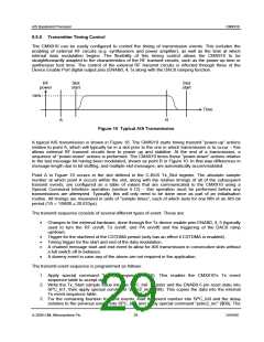
A working example of how to set up a transmit event sequence is shown in Table 2 (the order of events
and delay timings shown are for illustrative purposes only):
© 2009 CML Microsystems Plc
30
D/910/6

 CMLMICRO [ CML MICROCIRCUITS ]