AIS Baseband Processor
CMX910
5.5.5 Transmitter Timing Control
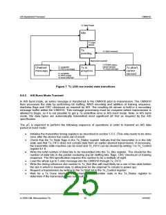
The CMX910 can be easily configured to control the timing of transmission events. This includes the
enabling of external RF circuits (e.g. synthesisers and power amplifier), as well as the time at which
internal data modulation begins. The flexibility of this timing control allows the CMX910 to be
straightforwardly adapted to the characteristics of the RF transmit circuits, such as the power up time or
synthesiser lock time. The control of the external RF transmit circuits is effected through three of the
Device Enable Port digital output pins (ENAB0, 4, 5) along with the DAC0 ramping function.
RF
Slot
Slot
power
start
start
100%
Time
A
B
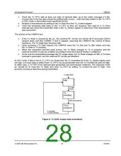
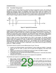
Figure 10 Typical AIS Transmission
A typical AIS transmission is shown in Figure 10. The CMX910 starts timing transmit “power-up” actions
relative to point A, which will typically be in a slot prior to the one in which transmission is to occur – this
allows external RF transmit circuits time to power up and stabilise. At the end of a transmission, a
sequence of “power-down” actions is performed. The CMX910 times these “power-down” actions relative
to the last message bit having been modulated, shown as point B in Figure 10. In that way differences in
message length due to bit stuffing, and multiple-slot messages, are automatically accommodated.
Point A in Figure 10 occurs in the slot defined in the C-BUS Tx_Slot register. The absolute sample
number at which point A occurs within the slot, along with the relative timings of all of the subsequent
transmit events, are configured as a table of values that are communicated to the CMX910 using a
Special Command Interface operation (section 5.12) – this operation must be performed before any
transmissions are attempted. Typically, this will only need to be done once as part of an initialisation
routine. All timings are measured in units of “sample times”, each of which lasts for one fifth of an AIS bit
period (1/5 × 1/9600 ≅ 20.833µs).
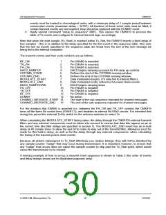
The transmit sequence consists of several different types of event. These are:
•
Changes to the external hardware, done through the Tx device enable pins ENAB0, 4, 5 (typically
used to turn the RF on/off, Tx on/off, and PA on/off) and the triggering of the DAC0 ramp
up/down.
•
•
•
Trigger for the start/end of the CSTDMA period (only has an effect if CSTDMA is enabled).
Timing trigger for the start and end of the data modulation.
A chained message start and end event to allow for AIS transmission in consecutive slots without
a full switch off in-between.
•
A dummy event in case any of the above are not required in the application.
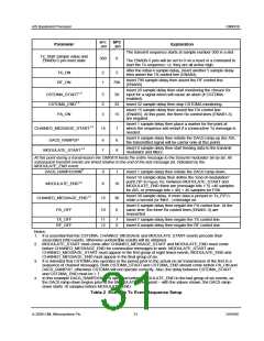
The transmit event sequence is programmed as follows:
1. Apply special command “load_tx_sequence” ($10). This readies the CMX910’s Tx event
sequence table to accept data.
2. Write the Tx_Start sample value into the SPC_In0 register and the ENAB0-5 pin reset state into
SPC_In1, then apply special command “poke2_inc” ($08). This copies the data into the internal
Tx event sequence table.
3. For the remaining fourteen transmit events, load the event number into SPC_In0 and the delay
(relative to the previous event) into SPC_In1, and apply special command “poke2_inc” ($08). The
© 2009 CML Microsystems Plc
29
D/910/6

 CMLMICRO [ CML MICROCIRCUITS ]