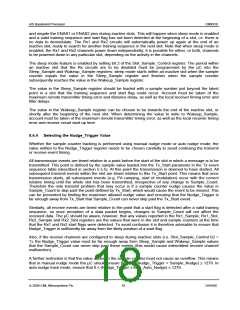
AIS Baseband Processor
CMX910
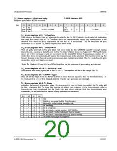
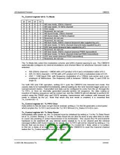
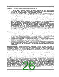
Tx_Control register b5-2: Tx Mode
b5
b4
b3
b2
0
0
0
0
0
0
0
0
1
1
1
1
1
1
1
1
0
0
0
0
1
1
1
1
0
0
0
0
1
1
1
1
0
0
1
1
0
0
1
1
0
0
1
1
0
0
1
1
0
1
0
1
0
1
0
1
0
1
0
1
0
1
0
1
AIS raw mode, 25kHz channel
AIS raw mode, 12.5kHz channel
DSC mode
Reserved, do not use
AIS burst mode, 25kHz channel
AIS burst mode, 12.5kHz channel
Reserved, do not use
Reserved, do not use
AIS test mode, 25kHz channel (transmit data supplied by µC)
AIS test mode, 12.5kHz channel (transmit data supplied by µC)
DSC test mode (transmit data supplied by µC)
Reserved, do not use
AIS test mode, 25kHz channel (internal PRBS transmitted)
AIS test mode, 12.5kHz channel (internal PRBS transmitted)
DSC test mode (internal PRBS transmitted)
Reserved, do not use
The Tx Mode bits select the modulation scheme and (AIS) channel spacing to use. The CMX910
automatically configures its internal modulators and channel filters for whichever transmit mode is
selected:
•
•
•
AIS (25kHz channel) = GMSK with a BT-product of 0.4 and a modulation index of 0.5.
AIS (12.5kHz channel) = GFSK with a BT-product of 0.3 and a modulation index of 0.25.
DSC = 1200 baud FSK, with frequency modulation of a 1700Hz sub-carrier and a pre-
emphasis of 6dB/octave. The frequency shift is between 1300Hz (logic 1) and 2100 Hz
(logic 0).
For both AIS and FSK operation, setting b5=1 puts the CMX910 into transmit test mode: this
causes data to be transmitted immediately, without waiting for the next transmit trigger point as in
normal transmit modes. Transmitted test data can be configured to come from the µC through the
Tx FIFO, or from an internally generated pseudo-random bit sequence. No data coding or
insertion of training sequences will be carried out, and the CMX910 will not attempt to perform RF
control using the ENAB pins and DAC0 ramping; transmission will continue until transmit test
mode is cleared by the µC. Note that when any test mode is enabled, it is essential that
Tx_Control b8 = 0.
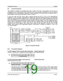
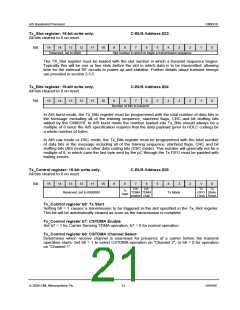
Tx_Control register b1: Tx FIFO Clear
Data written to this bit does not get stored; instead, writing a 1 to this bit generates a reset pulse
which empties the Tx FIFO and resets the Tx FIFO fill level (Tx_Status b13-8) to zero.
Tx_Control register b0: Tx State Reset
Immediately after power up, the Tx channel must be initialised by writing a 1 to the Tx State Reset
bit of Tx_Control. Writing a 1 to the Tx State Reset bit can also be done at any other time in order
to cause any pending or active transmission to be terminated – this causes the PA and transmit
hardware to be switched off, any internal states related to Tx to be cleared and the internal
message buffers (AIS burst mode) to be wiped. The Tx FIFO will not be cleared by writing a 1 to
this bit, that can be done if necessary by writing a 1 to Tx_Control bit 1. Note: when a 1 is written
to this bit, a delay of at least 250 µs is required for the CMX910 to reset the transmit channel
before the Tx_Control register is written to again.
© 2009 CML Microsystems Plc
22
D/910/6

 CMLMICRO [ CML MICROCIRCUITS ]