AIS Baseband Processor
CMX910
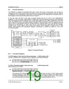
5.5
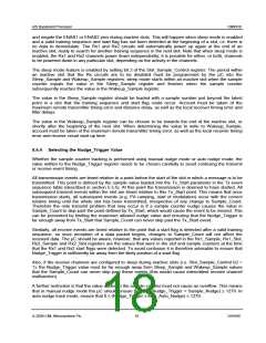
Transmit Operation
The CMX910 is capable of transmitting AIS data in either raw mode or burst mode, and can also be
configured for DSC transmission (FSK 1200 baud). AIS Carrier Sensing (CSTDMA) for Class B systems
is supported, as is a mechanism to allow two or more messages to be chained into consecutive slots. A
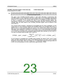
block diagram of the transmit data path is shown in Figure 6.
In AIS raw mode and DSC mode, data is passed directly from the Tx FIFO to the G(M)FSK/FSK
modulator, so the µC will be responsible for sending any necessary training sequence and performing
HDLC processing and NRZI coding for AIS, or other data coding for DSC. When configured in AIS burst
mode, the CMX910 uses a secondary internal message buffer to assemble an entire message (up to 5
slot) to which it automatically adds the training sequence, start/stop flags, CRC, bit stuffing and NRZI
coding prior to transmission. In either case, the µC must indicate how many data bits the message
contains in the Tx_Bits register, and in which slot to power up the external Tx circuits in the Tx_Slot
register. After setting up the appropriate registers, transmission is initiated by writing to a bit in the
Tx_Control register.
Reconstruction
C-BUS
filters
Tx_FIFO
(32 bytes)
HDLC/
NRZI
encoder
172 byte
message
buffer
I
Σ−Δ
DAC
ITXP
ITXN
AIS burst
G(M)FSK/
FSK
modulator
and filters
Q
AIS raw,
DSC
Σ−Δ
DAC
QTXP
QTXN
Tx_FIFO_Threshold
Tx_Status
Tx timing control
ENAB0
ENAB4
ENAB5
Tx_Slot
Tx_Bits
DAC ramp
Slot count
Sample count
Tx event
sequence
table
Tx_Control
CSTDMA_Threshold
Special command
interface
Figure 6 Transmit Channel
5.5.1 Transmitter Registers
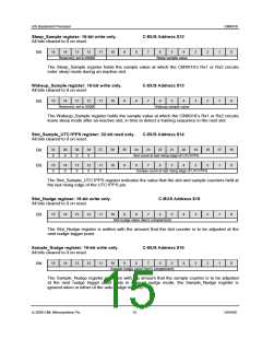
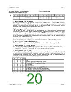
Tx_FIFO register: 8-bit write only (data-streaming). C-BUS Address $20
32 byte Tx channel FIFO, emptied on reset. Supports C-BUS data streaming.
7
6
5
4
3
2
1
0
Bit:
Tx channel data byte
Tx_FIFO_Threshold register: 8-bit write only.
C-BUS Address $21
All bits cleared to 0 on reset.
7
6
5
4
3
2
1
0
Bit:
Reserved, set to 000
Tx FIFO threshold level
The transmit FIFO threshold register is used to set the level at which a “FIFO nearly empty”
warning is triggered. If the number of bytes in Tx_FIFO is less than or equal to the value in bits 4-
0 of threshold register then the FIFO Trigger flag (bit 7 of Tx_Status) will be set to 1. This can also
be used to generate an interrupt. Bits 7-5 of TX_FIFO_Threshold should be set to 0.
© 2009 CML Microsystems Plc
19
D/910/6

 CMLMICRO [ CML MICROCIRCUITS ]