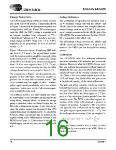
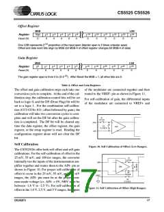
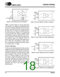
CS5525 CS5526
the input signal can be reduced to the point in
which the gain register reaches its upper limit of 2.0
(decimal) [FFFFFF Hex] (this is most likely to oc-
cur with an input signal approximately 1/2 the
nominal range). Alternatively, the input signal can
be increased to a point in which the modulator
reaches its one’s density upper limit of 80ꢀ (this is
most likely to occur with an input signal approxi-
mately 1.5 times the nominal range). Also, for full
scale inputs larger than the nominal full scale value
of the range selected, there is some voltage at
which the various internal circuits may saturate due
to limited amplifier headroom (this is most likely to
occur on the 100 mV range setting when NBV = -
1.8 V).
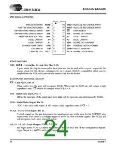
Serial Port Initialization
The serial port is initialized to the command mode
whenever a power-on reset is performed inside the
converter, when the port initialization sequence is
completed, or whenever a command byte, data
word sequence is completed. The port initialization
sequence involves clocking 15 (or more) bytes of
all 1's, followed by one byte with the following bit
contents (11111110). This sequence places the
chips in the command mode where it waits for a
valid command.
Performing Conversions (With PF bit = 0)
Setting the SC (Single Conversion) bit of the com-
mand word to a logic 1 with the CB bit = 1, all other
command bits = 0, the CS5525/CS5526 will per-
form one conversion. At the completion of the con-
version the DF (Done Flag) bit of the configuration
register will be set to a logic 1. The user can read
the configuration register to determine if the DF bit
is set. If DF has been set, a command can be issued
to read the conversion data register to obtain the
conversion data word. The DF bit of the configu-
ration register will be cleared to logic 0 when the
data register, the gain register, the offset register, or
the set-up registers are read. Reading only the con-
figuration register will not clear the DF flag bit.
Analog Output Latch Pins
The A3-A0 pins of the converters mimic the D23-
D20 bits of the configuration register. A3-A0 can
be used to control multiplexers and other logic
functions outside the converter. The outputs can
sink or source at least 1 mA, but it is recommended
to limit drive currents to less than 2 0µA to reduce
self-heating of the chip. These outputs are powered
from VA+, hence, their output voltage for a logic 1
will be limited to the VA+ voltage.
Serial Port Interface
If an SC command is issued to the converters while
they are performing a conversion, the filter will re-
start a convolution cycle to perform a new conver-
sion.
The CS5525/26 serial interface consist of four pins,
SCLK, SDO, SDI, and CS. The CS pin must be
held low (logic 0) before SCLK transitions can be
recognized by the port logic. The SDO output will
be held at high impedance any time CS is a logic 1.
Performing Conversions (With PF bit = 1)
If the CS pin is tied low, the port can function as a
three wire interface.
Setting the PF bit of the configuration register to a
logic 1 enables the SDO output pin to behave as a
The SCLK input is designed with a Schmitt-trigger flag signal whenever conversions are completed.
input to allow an optoisolator with slower rise and
fall times to directly drive the pin.
This eliminates the need for the user to read the DF
flag bit of the configuration register to determine if
the conversion data word is available.
The SDO output is capable of sinking or sourcing
up to 5 mA to directly drive an optoisolator LED.
If the SC (Single Conversion) command is issued
SDO will have less than a 400 mV loss in the drive (SC = 1, CB= 1, all other command bits = 0) the
voltage when sinking or sourcin g 5mA.
SDO pin will go low at the completion of a conver-
20
DS202F3

 CIRRUS [ CIRRUS LOGIC ]