CS5525 CS5526
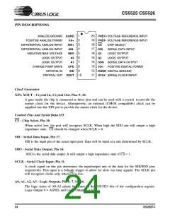
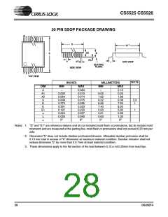
PIN DESCRIPTIONS
1
20
19
18
17
16
15
14
13
12
11
ANALOG GROUND AGND
VREF+ VOLTAGE REFERENCE INPUT
VREF- VOLTAGE REFERENCE INPUT
2
POSITIVE ANALOG POWER
DIFFERENTIAL ANALOG INPUT
DIFFERENTIAL ANALOG INPUT
NEGATIVE BIAS VOLTAGE
LOGIC OUTPUT
VA+
AIN+
AIN-
NBV
A0
3
CS
SDI
A3
CHIP SELECT
4
SERIAL DATA INPUT
LOGIC OUTPUT
LOGIC OUTPUT
5
6
A2
7
LOGIC OUTPUT
A1
SDO SERIAL DATA OUTPUT
VD+ POSITIVE DIGITAL POWER
DGND DIGITAL GROUND
8
CHARGE PUMP DRIVE
CRYSTAL IN
CPD
XIN
9
10
CRYSTAL OUT XOUT
SCLK SERIAL CLOCK INPUT
Clock Generator
XIN; XOUT - Crystal In; Crystal Out, Pins 9, 10.
A gate inside the chip is connected to these pins and can be used with a crystal to provide the
master clock for the device. Alternatively, an external (CMOS compatible) clock can be
supplied into the XIN pin to provide the master clock for the device.
Control Pins and Serial Data I/O
CS - Chip Select, Pin 18.
When active low, the port will recognize SCLK. When high the SDO pin will output a high
impedance state. CS should be changed when SCLK = 0.
SDI - Serial Data Input, Pin 17.
SDI is the input pin of the serial input port. Data will be input at a rate determined by SCLK.
SDO - Serial Data Output, Pin 14.
SDO is the serial data output. It will output a high impedance state if CS = 1.
SCLK - Serial Clock Input, Pin 11.
A clock signal on this pin determines the input/output rate of the data for the SDI/SDO pins
respectively. This input is a Schmitt trigger to allow for slow rise time signals. The SCLK pin
will recognize clocks only when CS is low.
A0, A1, A2, A3 - Logic Outputs, Pin 6, 7, 15, 16.
The logic states of A0-A3 mimic the states of the D20-D23 bits of the configuration register.
Logic Output 0 = AGND, and Logic Output 1 = VA+.
24
DS202F3

 CIRRUS [ CIRRUS LOGIC ]