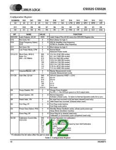
CS5525 CS5526
Charge Pump Drive
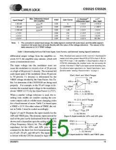
Voltage Reference
The CPD (Charge Pump Drive) pin of the convert- The CS5525/26 are specified for operation with a
ers can be used with external components (shown 2.5 V reference voltage between the VREF+ and
in Figure 1) to develop an appropriate negative bias
voltage for the NBV pin. When CPD is used to gen-
erate the NBV, the NBV voltage is regulated with
an internal regulator loop referenced to VA+.
VREF- pins of the devices. For a single-ended ref-
erence voltage, such as the LT1019-2.5, the refer-
ence’s output is connected to the VREF+ pin of the
CS5525/26. The ground reference for the LT1019-
Therefore, any change on VA+ results in a propor- 2.5 is connected to the VREF- pin.
tional change on NBV. With VA+ = 5 V, NBV’s
The differential voltage between the VREF+ and
regulation is set proportional to VA+ at approxi-
mately -2.1 V.
VREF- can be any voltage from 1.0 V up to 3.0 V,
however, the VREF- pin can not go below analog
ground.
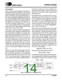
Figure 3 illustrates a means of supplying NBV volt-
age from a -5 V supply. For ground based signals
with the instrumentation amplifier engaged (when
in the 25mV, 55mV, or 100mV ranges), the voltage
on the NBV pin should at no time be less negative
than -1.8 V or more negative than -2.5 V. To pre-
vent excessive voltage stress to the chip the NBV
voltage should not be more negative than -3.0 V.
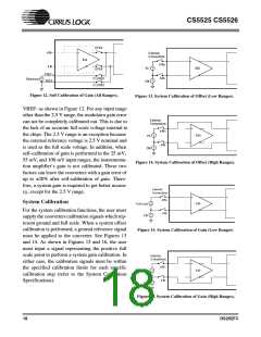
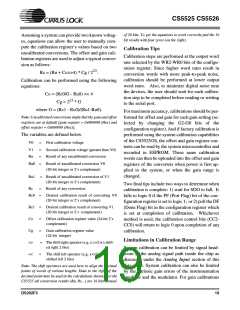
Calibration
The CS5525/26 offer five different calibration
functions including self calibration and system cal-
ibration. However, after the CS5525/26 are reset,
they can perform measurements without being cal-
ibrated. In this case, the converters will utilize the
initialized values of the on-chip registers (Gain =
1.0, Offset = 0.0) to calculate output words for the
±100 mV range. Any initial offset and gain errors
in the internal circuitry of the chips will remain.
The components in Figure 1 are the preferred com-
ponents for the CPD filter. However, smaller ca-
pacitors can be used with acceptable results. The
10 µF ensures very low ripple on NBV. Intrinsic
safety requirements prohibit the use of electrolytic
capacitors. In this case, two 0.47 µF ceramic capac-
itors in parallel can be used.
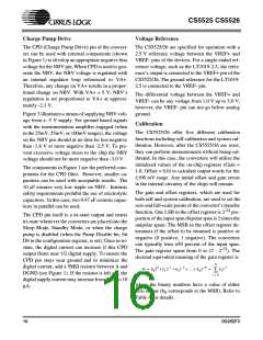
The gain and offset registers, which are used for
both self and system calibration, are used to set the
zero and full-scale points of the converter’s transfer
-24
function. One LSB in the offset register is 2 pro-
The CPD pin itself is a tri-state output and enters
tri-state whenever the converters are placed into the
Sleep Mode, Standby Mode, or when the charge
pump is disabled (when the Pump Disable bit, bit
D8 in the configuration register, is set). Once in tri-
state, the digital current can increase if this CPD
output floats near 1/2 digital supply. To ensure the
CPD pin stays near ground and to minimize the
digital current, add a 5MΩ resistor between it and
DGND (see Figure 1). If the resistor is left out, the
digital supply current may increase from 2 µA to 10
µA.
portion of the input span (bipolar span is 2 times the
unipolar span). The MSB in the offset register de-
termines if the offset to be trimmed is positive or
negative (0 positive, 1 negative). The converters
can typically trim 50 percent of the input span.
-23
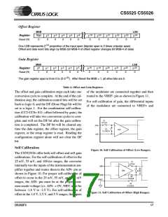
The gain register spans from 0 to (2 - 2 ). The
decimal equivalent meaning of the gain register is
N
D = b020 + b12–1 + b22–2 + … + bN2–N
=
bi2–i
∑
i = 0
where the binary numbers have a value of either
zero or one (b corresponds to the MSB). Refer to
0
Table 4 for details.
16
DS202F3

 CIRRUS [ CIRRUS LOGIC ]